
Solder Joint Volume and Pad Geometry
Solder joint volume is one of the few characteristics of an assembly that is decided at the design stage and then reproduced, or not, by the process. The land pattern sets how much solder the joint can hold, the paste deposit sets how much is offered, and the reflow decides how it distributes itself. Get the geometry wrong and no amount of process control will produce a reliable joint; get it right and the process window becomes wide enough to run comfortably.
What Determines Joint Volume
The volume of a surface mount joint is the sum of the paste deposit volume, minus what is lost to flux and to volatiles, plus the solder already present as plating on the pad and the termination. For a chip component the plating contribution is small; for a component with a thick hot-air levelled finish or a solder-coated lead it can be a significant fraction. The deposit is therefore the design lever, and the land pattern decides how much of it stays where it is wanted.
The pad area also sets the shape of the fillet. A pad that extends well beyond the termination allows the solder to form a long, low fillet that adds little strength; a pad that is only slightly larger than the termination concentrates the solder into a tall fillet that is stronger but that may not form if the volume is short. The relationship between pad extension and fillet height is what the land pattern standards are built on.
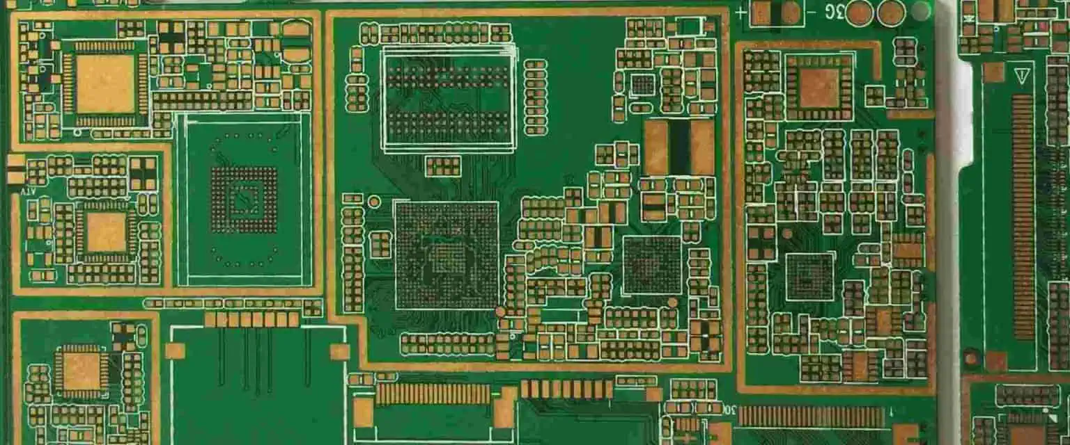
Land Pattern and Its Effect on the Fillet
The land pattern defines the pad length, the pad width and the spacing, and the extension beyond the component termination is the parameter that most affects the fillet. A typical extension is a fraction of a millimetre for a chip component and a small multiple of the lead width for a gull-wing device. Reducing the extension concentrates the solder and produces a higher fillet; increasing it spreads the solder and lowers the fillet for the same volume.
The pad width matters for the same reason. A pad that is wider than the termination allows the solder to spread sideways, which lowers the fillet height and can produce a joint that looks starved even though the volume is correct. A pad that is too narrow constrains the solder and produces a fillet that is tall but narrow, which is harder to inspect and more likely to have a void at the heel.
Paste Deposit Volume and the Stencil
The deposit volume is set by the aperture area and the foil thickness, so the stencil is the tool that connects the design intent to the process. A design that needs more solder can be served by a thicker foil or a larger aperture, and the two have different consequences: a thicker foil reduces the area ratio and complicates the release, while a larger aperture changes where the deposit sits and can move it closer to the mask.
The deposit volume should be calculated for the critical joints rather than assumed. The calculation is the aperture area multiplied by the foil thickness and by a transfer efficiency that is less than one for small apertures. Where the calculated volume is below the requirement, the design should be examined before the foil is changed, because a land pattern that is too small will not be fixed by more paste. The paste volume figures and the aperture design rules give the working numbers.

Through-Hole Joint Volume and Barrel Fill
A through-hole joint has to fill the barrel as well as form a fillet on both sides, so its volume requirement is far larger than a surface mount joint of the same footprint. The volume comes from the annular gap between the lead and the hole wall, multiplied by the board thickness, plus the two fillets. Where the gap is large, the volume needed rises quickly, which is why a hole that is generously sized for insertion becomes difficult to fill.
The plating thickness in the barrel contributes to the fill, and a heavily plated hole needs slightly less solder. Where the joint is made by a wave, the volume is supplied continuously and the limiting factor is the hole-to-lead clearance and the thermal profile. Where the joint is made by printed paste, the volume has to be printed, and the relationship between the aperture, the foil and the required volume sets the limit. The hole copper figures are part of the calculation, because the plating reduces the gap the solder has to fill.
Too Much Solder and Its Consequences
Excess solder raises the fillet beyond the point where it adds strength and starts to add risk. A very tall fillet on a chip component can bridge to a neighbouring joint, and it reduces the clearance for a conformal coating. On a fine-pitch device, excess solder on one lead can reach the adjacent lead during reflow and form a bridge that surface tension alone will not pull apart.
Excess also hides defects. A joint with a large solder volume can conceal a poor wetting at the pad, because the visible fillet forms from the solder above rather than from the interface. Where the design allows a large volume, the inspection becomes less able to judge the property that matters, which is the reason the standards limit the fillet height as well as the minimum coverage.
Too Little Solder and Its Consequences
Insufficient solder produces a joint that is mechanically weak even when it is electrically continuous. The failure appears later, after thermal cycling or vibration, as a crack at the interface or at the heel of the fillet. The joint may pass an electrical test and pass a visual inspection under poor light, which is why the minimum fillet requirement is written as a visible fillet rather than as a resistance limit.
The shortage can come from the design, from the stencil or from the process. A deposit that is correct but sits partly on the mask does not contribute to the joint; a pad that is too small cannot hold what is offered; a reflow profile that wicks solder into a via or onto a neighbouring feature takes it away from the joint. Separating those causes needs a cross-section of a suspect joint, which shows the volume actually present rather than the volume that was printed.
Designing the Land Pattern for the Volume
The land pattern should be designed for the volume requirement and then verified against the process. Starting from the component maker’s recommended pattern is the right approach, and the recommendation should be checked against the volume the joint needs rather than accepted as a formality. Where a pattern is derived from a similar part with a different termination geometry, the volume requirement may not transfer, and the first article will show it.
The pattern should also respect the process limits. A pattern that requires a deposit with an area ratio below the practical minimum is not manufacturable at a reasonable yield, and the design should be changed rather than the process pushed. Where the pattern is tight, the layout for soldering yield notes describe the adjustments that make the difference between a marginal and a robust joint.
Verification by Cross-Section
A cross-section is the definitive check on joint volume, because it measures what is present rather than what was printed. The section should be taken through the middle of a representative joint and should include the pad, the termination and the fillet. The measurements that matter are the fillet height at the toe and the heel, the wetting along the pad, and the presence of voids or intermetallic growth beyond the normal thickness.
Sectioning is destructive, so it is used at the first article and on samples from a production lot rather than on production units. The result should be recorded with the joint geometry so that a later comparison is possible. Where the section shows a shortfall, the corrective action should follow the cause: the deposit, the pad or the profile. Changing the paste or the profile when the pad is too small is a common and expensive mistake, and the section is what distinguishes the two cases.
Additional Considerations for This Build
Practical attention to pad geometry pays for itself here, because it decides whether the finished board behaves as the drawing intended. Where the requirement is not stated on the fabrication drawing or in the assembly notes, the shop has to assume a default, and that default is rarely the value the design was simulated with. Stating pad geometry explicitly, together with the tolerance that applies, removes the assumption and keeps the result predictable from batch to batch.
Deliberate attention to solder fillet pays for itself here, because it decides whether the finished board behaves as the drawing intended. Where the requirement is not stated on the fabrication drawing or in the assembly notes, the shop has to assume a default, and that default is rarely the value the design was simulated with. Stating solder fillet explicitly, together with the tolerance that applies, removes the assumption and keeps the result predictable from batch to batch.
FAQ
Can a joint be too small to see but still be acceptable? A joint with no visible fillet is not acceptable on a product that will see thermal cycling or vibration, regardless of its electrical continuity. The minimum fillet requirement exists because the mechanical property, not the electrical one, is what fails first.
Does a thicker stencil always give more solder? It gives a larger deposit only if the aperture can release it. As the foil thickens, the area ratio falls, and below the practical limit the aperture retains paste instead of transferring it, so the deposit volume falls rather than rises.
How much does the pad plating contribute? For a hot air levelled finish or a solder-coated lead it can be a meaningful fraction of the total. For a thin gold or silver finish it is negligible. The contribution should be included where the volume is marginal.