Via Plugging vs Tenting: What Solder Mask Should Do to a Via
The decision about what solder mask should do to a via is usually made in a single line on the fabrication drawing, and it decides whether the assembly line sees a sealed surface or a row of open barrels. Tenting, mask plugging and resin plugging are three different processes with three different failure modes, and the choice follows from what the via has to do rather than from what the fabricator normally supplies. This article sets out the geometry, the cure variables and the tests that prove the result.
What Tenting Covers and Where It Fails
Tenting leaves the solder mask film intact across the via opening, so the mask bridges the hole instead of forming a ring around it. A 0.3 mm via under a 25 micrometre dry film is usually covered without difficulty, but the film thins over the hole and the solvent released during cure can leave a blister at that point.
The failure appears at reflow rather than at fabrication. Air and moisture trapped in the barrel expand above 200 degrees Celsius, and the pressure lifts the mask until it ruptures, leaving a crater that collects flux and produces solder balls on the far side of the board.
Solder Mask Plugging from the Print Side
Mask plugging pushes the same resist through the barrel with a squeegee, usually in two passes with a blade of 60 to 75 durometer and a print speed slow enough to let the material fill the hole. Vacuum assistance from below the panel pulls resist through and improves fill on high aspect ratio vias, where the print alone leaves the barrel partly empty. Barrel geometry itself is covered in our hole copper notes.
Cure shrinkage governs the result. An epoxy based mask loses two to five percent of its volume during cure, so a via that is filled flush at print time can finish with a dimple of 10 to 25 micrometres. That is acceptable for a via that carries no paste and not acceptable for a via that sits inside a thermal pad.
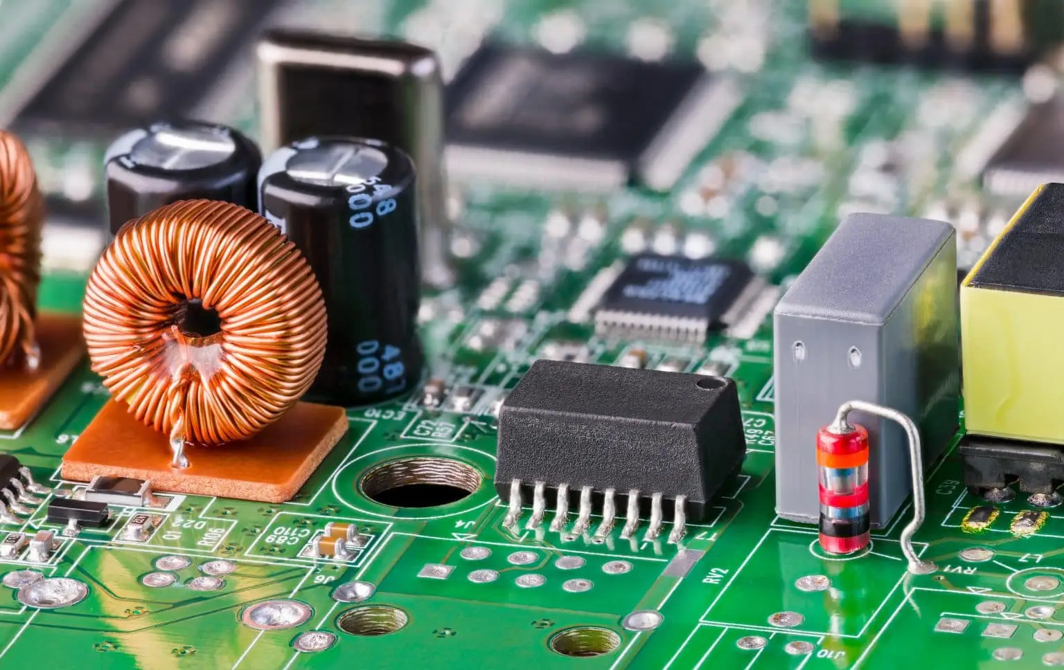
Fill depth is measured by microsection rather than by looking at the surface, because a plug that reaches only part of the barrel looks identical to a full one from above.
Resin Plugging and Planarisation
Resin plugging, the most demanding form of via plugging, uses a dedicated epoxy applied by stencil or dispenser, cured, and then ground back until the surface is coplanar with the copper. The planarisation step is what makes the process usable for via in pad, and it is controlled to a flatness of about 25 micrometres across the pad.
The resin has to be cured before grinding, and the schedule matters because a partial cure smears rather than cuts while an over cured plug becomes brittle and chips at the pad edge. Typical schedules sit between 150 degrees Celsius for 60 minutes and 170 degrees for 30 minutes, and the supplier data should be followed rather than approximated.
Requirements for Via in Pad
A via inside a BGA pad has to be filled and capped with plating, and both the dimple depth and the cap thickness are specified. A dimple deeper than 25 micrometres holds paste away from the joint and creates a void, while a cap thinner than 5 micrometres can crack during thermal cycling.
The plating cap adds 5 to 8 micrometres of copper over the plug on most processes, and that copper belongs in the impedance and current calculations when the via sits on a controlled impedance net. The fabricator should confirm both numbers on a microsection rather than by inspecting the surface.
Voiding above a plugged via is judged on the X-ray image of the joint, and the same pad should be compared before and after a bake to separate a material problem from a profile problem.
Outgassing, Voiding and the Reflow Path
Any material left in the barrel that has not been fully cured releases volatiles as the assembly passes through the oven. The consequence is a void in the solder joint above the via, and the void is largest when paste is printed directly over an incompletely filled hole.
The measurement that separates a material problem from a profile problem is void percentage from X-ray taken before and after a bake. If a two hour bake at 125 degrees Celsius reduces the void area, the plug was under cured; if it does not, the profile or the paste is responsible.
Testing and Acceptance
Plugged and tented vias are verified by microsection, by X-ray for the joints above them, and by dye and pry where adhesion is in question. Microsection is the only method that shows dimple depth, cap thickness and void content in the plug at the same time, and it should be taken from a production panel rather than a hand prepared coupon.
For assemblies qualified by thermal cycling, the acceptance figure is a change in resistance rather than a visual result. A daisy chained via that shifts by more than a few percent after 100 cycles between minus 40 and 125 degrees Celsius indicates a plug that has cracked or a cap that has separated. The fixtures used for that work are described in our notes on thermal cycling test design.
Consequences for Assembly Yield
An open via beside a fine pitch pad wicks paste away from the joint during reflow. The paste that leaves the pad is no longer available to form the fillet, and the result is a joint with insufficient volume that can still pass X-ray because a ball is present but thinner than the print suggested.
On the second side of a double sided assembly the same open via lets solder pass through to the first side, where it forms a ball on a surface that may already be populated or coated. Tenting and plugging both remove that path, and the choice between them normally follows from whether the via sits on a pad. Inspecting the result is covered in our guide to X-ray and AOI.
Interaction with the Surface Finish
Hot air solder levelling is incompatible with plugged vias, because molten alloy is blown out of the barrel and the plug is disturbed by the air knife. The same applies to any finish applied after the mask cure, so plugging is normally paired with ENIG, immersion silver or another chemical finish.
Where ENIG is used over a plugged via, the nickel and gold deposit onto the copper cap, and the chemistry has to be controlled so that the plug boundary does not become a corrosion site. Gold at 0.05 to 0.1 micrometres over nickel at 3 to 6 micrometres is checked on a coupon that includes vias, following the methods in our plating thickness guide.
Cost, Documentation and Choice
Tenting costs nothing beyond the mask artwork, mask plugging adds a print step, and resin plugging adds print, cure, planarisation and a second cure, which makes it the most expensive option per panel. The decision therefore follows the function of the via rather than a general preference for one process.
The drawing should say which vias are plugged and which are tented, whether the plug has to be electrically conductive, the maximum dimple and the minimum cap thickness. Where a via sits inside a pad, the via structure belongs in the stack-up drawing, where it can be checked before the panel is released for fabrication.
FAQ
Can a tented via replace a plugged one? Only where the via carries no paste and no thermal pad sits over it. Tenting closes the barrel well enough for a signal via, but it does not provide a surface that paste can be printed onto.
How deep may a dimple be? Twenty five micrometres is the usual limit for a via in pad. Deeper dimples hold paste away from the joint and are a common source of voids that appear only after X-ray.
Does plugging change the impedance of the via? The plating cap adds copper around the barrel, which slightly lowers inductance and changes the local geometry, so both the cap thickness and the finished hole size should be shown on the controlled impedance drawing.