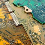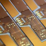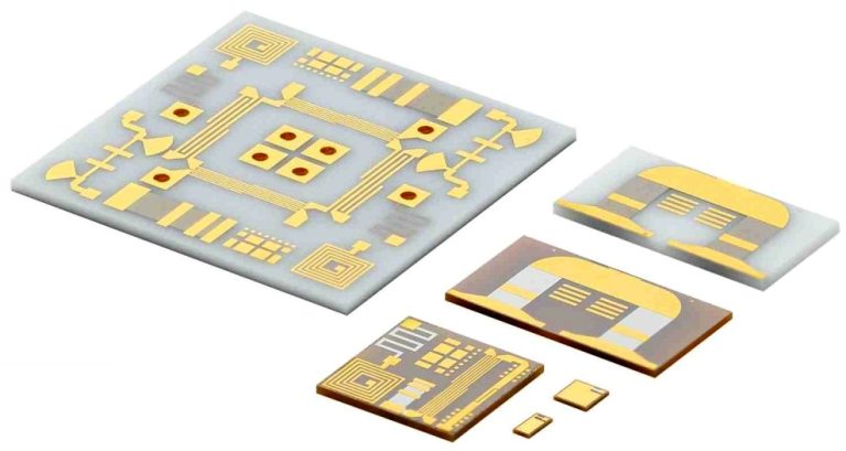
A Ceramic PCB is a printed circuit board that uses a ceramic substrate instead of conventional organic materials such as FR-4. Ceramic substrates are valued for their excellent thermal performance, electrical insulation, dimensional stability, and resistance to demanding operating environments.
Common ceramic substrate materials include alumina (Al₂O₃), aluminum nitride (AlN), and beryllium oxide (BeO). Depending on the required electrical, thermal, and mechanical performance, different ceramic materials and metallization technologies can be selected.
Unlike conventional organic PCBs, a Ceramic PCB Substrate can provide significantly higher thermal conductivity and better stability at elevated temperatures. This makes ceramic circuit boards particularly suitable for high-power electronics, power modules, RF and microwave systems, LEDs, automotive electronics, aerospace equipment, and other applications where efficient heat dissipation is critical.
Another important parameter is the coefficient of thermal expansion (CTE). CTE describes how much a material changes in size as its temperature changes. Because electronic assemblies experience repeated heating and cooling, matching the thermal expansion characteristics of the substrate, copper conductors, and semiconductor components is important for long-term reliability.
Key Characteristics of Ceramic PCB
1. High Thermal Conductivity
One of the most important advantages of a Ceramic PCB is its excellent thermal performance.
Materials such as alumina and especially aluminum nitride can provide substantially higher thermal conductivity than standard FR-4. This allows heat generated by power semiconductors, LEDs, RF devices, and other components to move more efficiently away from the heat source.
Effective thermal management can help reduce operating temperature, improve component reliability, and support higher power density.
2. Excellent Electrical Insulation
Ceramic materials are excellent electrical insulators.
A Ceramic PCB Substrate can electrically isolate conductive copper structures while maintaining strong thermal performance. This combination of electrical insulation and heat dissipation is particularly valuable in power electronics.
Ceramic substrates are also suitable for high-voltage applications when the substrate thickness, dielectric strength, creepage distance, clearance, and overall design are properly selected.
3. Excellent Thermal Stability
Ceramic materials can maintain their mechanical and electrical characteristics over a wide temperature range.
This makes Ceramic PCB technology suitable for applications exposed to elevated temperatures, thermal cycling, and demanding operating conditions.
The actual operating temperature capability depends on the ceramic material, metallization system, assembly structure, and application environment.
4. Low and Stable Thermal Expansion
The CTE of a ceramic substrate can be relatively low and stable compared with many organic PCB materials.
This can help reduce mechanical stress caused by temperature changes, particularly when the ceramic substrate is integrated with semiconductor devices.
For high-reliability power modules, selecting a substrate with suitable CTE characteristics can improve the reliability of solder joints, metallization layers, and semiconductor interfaces.
5. Chemical and Environmental Resistance
Ceramic materials generally provide strong resistance to moisture, chemicals, corrosion, and harsh environmental conditions.
This makes ceramic substrates useful in applications where conventional organic PCB materials may have difficulty maintaining long-term performance.
Potential applications include industrial equipment, outdoor electronics, aerospace systems, power electronics, and other harsh-environment systems.
6. High Mechanical Rigidity
Ceramic substrates have high stiffness and can maintain their shape under normal operating conditions.
This rigidity can be advantageous for applications requiring stable dimensions and precise conductor positioning.
However, ceramic is also relatively brittle compared with organic laminates. Mechanical shock, excessive bending, or improper handling can cause cracking, so ceramic boards require appropriate mechanical design and manufacturing processes.
How Is a Ceramic PCB Manufactured?
The Ceramic PCB Manufacturing process differs from conventional FR-4 PCB fabrication because the substrate and metallization technologies are different.
The exact manufacturing process depends on the ceramic material and the selected metallization method.
Step 1: Ceramic Substrate Preparation
Ceramic substrates commonly start with ceramic powders such as alumina or aluminum nitride.
The powder is processed into a suitable ceramic green body using techniques such as tape casting, pressing, or other forming processes.
For multilayer ceramic technologies, the ceramic layers can be prepared separately and then processed together according to the required structure.
Step 2: Ceramic Sintering
The formed ceramic material is heated under controlled conditions to remove binders and densify the ceramic.
The sintering temperature depends strongly on the material and manufacturing technology.
For example, alumina and aluminum nitride require high-temperature processing, while LTCC uses specially formulated glass-ceramic materials that can be cofired at substantially lower temperatures.
Step 3: Metallization
After or during ceramic processing, conductive metal structures are formed on the substrate.
Depending on the technology, metallization may use:
- Thick-film technology
- Thin-film technology
- Direct Bonded Copper (DBC)
- Direct Copper Plating (DPC)
- Laser Activated Metallization (LAM)
- Other specialized metallization processes
The choice depends on conductor thickness, resolution, thermal performance, current capacity, and application requirements.
Step 4: Circuit Pattern Formation
The required copper or metal circuit pattern is created according to the PCB design.
Depending on the selected process, photolithography, screen printing, plating, etching, laser processing, or other patterning technologies may be used.
Step 5: Drilling and Via Formation
Depending on the ceramic PCB structure, holes and vias may be created through mechanical drilling, laser processing, or specialized ceramic processing methods.
Via formation is especially important for multilayer ceramic substrates and high-density interconnect structures.
Step 6: Surface Finishing
The exposed conductive areas may receive an appropriate surface finish or metallization treatment depending on the assembly process.
The selected finish should provide the required solderability, contact reliability, corrosion resistance, and service life.
Step 7: Inspection and Testing
The finished ceramic board undergoes inspection and testing.
Depending on the application, this can include:
- Visual inspection
- Dimensional inspection
- Electrical continuity testing
- Isolation testing
- Thermal inspection
- Metallization inspection
- X-ray inspection
- Reliability testing
High-power and high-reliability applications may require additional thermal cycling, temperature-humidity, mechanical, or electrical reliability testing.
Types of Ceramic PCB
Ceramic PCBs can be classified according to both substrate material and manufacturing technology.
Ceramic PCB Types by Material
1. Alumina Ceramic PCB
Alumina (Al₂O₃) is one of the most widely used ceramic substrate materials.
It provides good electrical insulation, thermal performance, mechanical strength, and cost effectiveness.
Because of its balanced characteristics, alumina is widely used in power electronics, LED modules, sensors, RF components, and industrial electronics.
2. Aluminum Nitride PCB
Aluminum nitride (AlN) provides significantly higher thermal conductivity than standard alumina.
Its CTE is also relatively close to that of silicon, which can be advantageous in semiconductor packaging and high-power applications.
Aluminum Nitride PCB technology is therefore often considered for high-power modules, laser systems, RF devices, and advanced thermal-management applications.
3. Beryllium Oxide PCB
Beryllium oxide (BeO) has excellent thermal conductivity combined with strong electrical insulation.
However, beryllium-containing materials require strict industrial health and safety controls during manufacturing and handling because beryllium compounds can pose serious health risks.
For this reason, BeO is generally reserved for specialized applications where its performance advantages justify the additional handling requirements.
4. Boron Nitride Ceramic PCB
Boron nitride offers excellent thermal characteristics and electrical insulation.
It can be used in specialized thermal-management and high-temperature applications where conventional PCB substrates are insufficient.
5. Silicon Carbide Ceramic PCB
Silicon carbide has excellent high-temperature and environmental resistance.
It is particularly relevant to specialized power electronics and extreme-environment applications.
Ceramic PCB Types by Manufacturing Technology
1. Thick-Film Ceramic PCB
Thick-film technology forms conductive, resistive, or dielectric patterns on a ceramic substrate using printed functional pastes.
The material is then fired to create the required electrical structure.
Thick-film ceramic substrates can integrate resistors and other passive functions, which can help reduce assembly complexity and component count in suitable applications.
2. Thin-Film Ceramic PCB
Thin-film technology uses processes such as sputtering, evaporation, photolithography, and electroplating to create precise metal patterns on ceramic substrates.
Compared with conventional thick-film processing, thin-film technology can achieve finer conductor geometries and is therefore useful for high-density and high-frequency applications.
3. Hybrid Ceramic PCB
A hybrid ceramic PCB combines ceramic and other substrate materials or technologies within the same assembly.
The objective is to combine the advantages of different materials, such as thermal performance in selected regions and conventional PCB routing or mechanical characteristics in others.
The exact hybrid structure must be designed according to the electrical, thermal, mechanical, and manufacturing requirements.
4. Low-Temperature Cofired Ceramic (LTCC)
LTCC uses specially formulated glass-ceramic materials that can be cofired with compatible conductive materials at relatively low temperatures compared with traditional high-temperature ceramic processing.
Multiple ceramic layers can contain conductive patterns and vias before they are laminated and cofired.
LTCC is widely associated with compact multilayer ceramic circuits, RF modules, filters, antennas, sensors, and other miniaturized electronic structures.
5. High-Temperature Cofired Ceramic (HTCC)
HTCC uses ceramic materials such as alumina and conductive materials that can withstand high-temperature firing.
Multiple ceramic layers can be stacked and cofired to form multilayer circuits with embedded conductors and vias.
HTCC is used in applications requiring high-temperature stability, mechanical robustness, hermetic packaging, and reliable electrical performance.
6. Direct Bonded Copper (DBC) Ceramic PCB
DBC PCB technology bonds copper directly to a ceramic substrate through a controlled high-temperature bonding process.
Common substrate materials include alumina and aluminum nitride.
The resulting structure provides:
- High thermal conductivity
- Strong electrical insulation
- High current-carrying capability
- Low electrical resistance
- Good mechanical stability
DBC is widely used in power semiconductor modules, power converters, motor drives, electric vehicles, renewable-energy systems, and other high-power applications.
7. Direct Plated Copper (DPC) Ceramic PCB
DPC PCB technology uses a plating-based metallization process to form copper structures directly on a ceramic substrate.
Compared with DBC, DPC can provide finer circuit patterns and is suitable for applications requiring higher pattern resolution.
DPC technology is frequently used for LED packages, semiconductor devices, RF components, and high-density ceramic circuits.
8. Laser Activated Metallization (LAM)
LAM uses laser processing to selectively activate and structure the ceramic surface before subsequent metallization.
This technology can support the formation of fine conductive patterns on ceramic substrates.
It is particularly attractive for applications requiring high-resolution metallization and advanced ceramic interconnect structures.
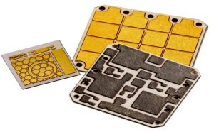
DPC vs. DBC Ceramic PCB
DPC and DBC are both important ceramic metallization technologies, but their manufacturing principles and typical applications are different.
| Feature | DPC | DBC |
|---|---|---|
| Basic principle | Plated copper metallization | Direct copper-to-ceramic bonding |
| Circuit resolution | Generally finer | Generally optimized for thicker copper and power structures |
| Copper thickness | Suitable for relatively fine and controlled structures | Often suitable for thick copper power applications |
| Typical applications | LEDs, RF, semiconductor packaging | Power modules, inverters, motor drives |
| Main advantage | Fine pattern capability | High current and thermal performance |
The appropriate technology depends on copper thickness, circuit resolution, thermal requirements, electrical current, and assembly structure.
Applications of Ceramic PCB
The combination of thermal performance, electrical insulation, and environmental stability makes Ceramic PCB Applications particularly important in demanding electronic systems.
1. Power Electronics
Ceramic substrates are widely used in high-power modules, power converters, motor drives, and semiconductor packages.
Their thermal performance allows heat to move efficiently from power devices toward the cooling structure.
2. LED Lighting
High-power LEDs generate substantial heat.
Ceramic substrates can provide an effective thermal path while maintaining electrical insulation, making them suitable for high-power LED packages and lighting modules.
3. RF and Microwave Electronics
Ceramic materials can provide stable electrical characteristics and low-loss performance depending on the selected material and structure.
They can therefore be used in RF modules, microwave circuits, communication components, filters, and antenna-related applications.
4. Automotive Electronics
Ceramic substrates can be used in automotive power electronics, LED lighting, sensors, power modules, and other systems exposed to thermal cycling and demanding operating conditions.
5. Aerospace and Defense
Ceramic circuit technologies can be used in aerospace and defense electronics where thermal stability, environmental resistance, reliability, and compact packaging are important.
Typical applications include RF modules, sensors, power electronics, and specialized electronic packages.
6. Renewable Energy Systems
Ceramic substrates are used in selected solar power, energy storage, power conversion, and inverter applications.
Their thermal and electrical characteristics can support high-power semiconductor devices used in energy systems.
7. Semiconductor Packaging
Ceramic substrates are widely used in advanced electronic packaging because they can combine electrical insulation, thermal conduction, mechanical rigidity, and dimensional stability.
8. Industrial Equipment
Industrial power supplies, motor drives, sensors, control systems, and high-temperature equipment can use ceramic substrates when standard organic PCB materials cannot provide sufficient thermal or environmental performance.
Advantages of Ceramic PCB Compared with FR-4
The main differences between ceramic and conventional FR-4 substrates are related to thermal and environmental performance.
| Characteristic | Ceramic PCB | FR-4 PCB |
|---|---|---|
| Thermal conductivity | High to very high, depending on material | Relatively low |
| Electrical insulation | Excellent | Excellent |
| High-temperature stability | Excellent | Depends on laminate grade |
| Moisture resistance | Generally excellent | Moderate |
| Mechanical rigidity | High | Good |
| Brittleness | Relatively high | Lower |
| High-power thermal management | Excellent | Limited |
| Cost | Generally higher | Generally lower |
| Typical use | Power, RF, LED, harsh environments | General electronics |
Ceramic does not automatically outperform FR-4 in every category. FR-4 remains the more economical and versatile choice for many standard PCB applications.
Design Considerations for Ceramic PCB
When designing a Ceramic PCB, several factors should be evaluated at the beginning of the project.
1. Select the Appropriate Ceramic Material
Alumina, aluminum nitride, and other ceramics offer different combinations of thermal conductivity, CTE, dielectric properties, mechanical strength, and cost.
The material should be selected according to the actual application.
2. Consider Thermal Expansion
The CTE relationship between the ceramic substrate, copper metallization, solder, and semiconductor devices should be evaluated.
This is particularly important for applications exposed to repeated thermal cycling.
3. Optimize Thermal Paths
Power components should be positioned and connected to provide an efficient thermal path.
Copper thickness, thermal interfaces, heat sinks, and mounting structures should be considered together with the ceramic substrate.
4. Control Mechanical Stress
Ceramic is rigid but relatively brittle.
The PCB design should avoid unnecessary mechanical stress, excessive bending, concentrated mounting stress, and inappropriate handling conditions.
5. Select the Right Metallization Technology
DBC, DPC, thick-film, thin-film, LTCC, HTCC, and LAM technologies have different capabilities.
The selection should be based on conductor thickness, resolution, current requirements, thermal performance, and production volume.
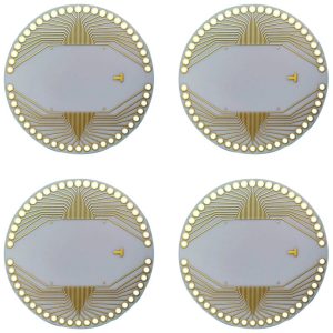
Kingda: Ceramic PCB Manufacturing Solutions
Kingda provides PCB manufacturing solutions for customers requiring specialized circuit-board technologies, including applications where thermal management, electrical insulation, high-frequency performance, and environmental stability are important.
For ceramic PCB projects, engineering evaluation should consider the substrate material, copper or metallization structure, circuit resolution, thermal requirements, CTE compatibility, surface finish, and assembly process.
Kingda can work with customers to evaluate the appropriate Ceramic PCB Substrate and manufacturing approach according to the requirements of the final electronic system.
For high-power, RF, LED, automotive, industrial, and other demanding applications, selecting the appropriate ceramic material and manufacturing technology at the design stage can help improve thermal performance, reliability, and overall product efficiency.
Conclusion
A Ceramic PCB is a specialized circuit-board technology designed for applications where conventional organic PCB materials may not provide sufficient thermal, electrical, or environmental performance.
Alumina, aluminum nitride, and other ceramic materials provide excellent electrical insulation and thermal stability, while technologies such as DBC, DPC, thick-film, thin-film, LTCC, HTCC, and LAM enable different circuit structures and performance levels.
The main advantage of ceramic substrates is their ability to combine electrical insulation with strong thermal performance. This makes them particularly valuable for high-power electronics, LED modules, RF and microwave systems, semiconductor packaging, automotive electronics, aerospace equipment, and demanding industrial applications.
However, ceramic materials are generally more expensive and more brittle than conventional FR-4. Therefore, material selection and manufacturing technology should be based on the actual electrical, thermal, mechanical, and reliability requirements of the product.
With appropriate material selection, thermal design, metallization technology, and manufacturing process control, Ceramic PCB Manufacturing can provide a reliable solution for advanced electronic systems where efficient heat dissipation and long-term stability are critical.