What Is an IC Substrate PCB?
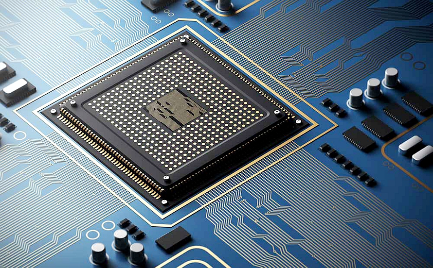
An IC Substrate PCB is a high-density interconnection substrate used as the fundamental interface between an integrated circuit (IC) package and a conventional printed circuit board (PCB). It provides electrical connections, mechanical support, signal routing, power distribution, and thermal management between the semiconductor die and the system-level PCB.
Compared with conventional PCBs, an IC Substrate requires significantly finer circuit patterns, smaller pad dimensions, tighter dimensional tolerances, and more precise manufacturing processes. It can be considered a highly miniaturized interconnection platform similar in concept to an HDI PCB, but designed specifically to meet the requirements of advanced semiconductor packaging.
IC substrates are widely used in package technologies such as BGA, CSP, flip-chip, and other high-density semiconductor packages. As semiconductor devices continue to become smaller and more powerful, the substrate must provide increasingly dense interconnections while maintaining signal integrity and thermal reliability.
The primary purpose of IC Packaging is to protect the semiconductor die while providing reliable electrical and mechanical connections to the external system. The IC substrate serves as an intermediate layer between the tiny connections on the chip and the larger connection structure of the PCB.
Modern IC substrates are commonly used in processors, memory devices, graphics processors, communication chips, networking equipment, smartphones, tablets, medical electronics, aerospace systems, and other high-performance electronic products.
What Is the Role of an IC Substrate?
An IC Substrate performs several critical functions within an advanced semiconductor package:
- Provides electrical interconnection between the semiconductor die and PCB.
- Converts the fine-pitch connections of an IC into a larger external package interface.
- Distributes power and ground to the semiconductor device.
- Routes high-speed signals while minimizing signal loss and crosstalk.
- Provides mechanical support for the semiconductor die.
- Helps dissipate heat generated during device operation.
- Protects the semiconductor package from environmental and mechanical stresses.
For system-on-chip (SoC) devices, the substrate can accommodate high-density routing for integrated GPIOs, memory interfaces, high-speed communication channels, and other peripheral connections.
Because the electrical distance between the IC and substrate is extremely short, the substrate design has a direct impact on impedance, parasitic effects, signal integrity, and overall package performance.
Types of IC Substrate PCBs
Different IC Substrate PCB structures are designed according to package architecture, electrical requirements, thermal performance, manufacturing technology, and cost.
BGA IC Substrate
BGA substrates are commonly used for processors, application processors, GPUs, and other high-performance ICs with a large number of external connections.
BGA packages can accommodate hundreds of solder balls and provide a relatively high interconnection density. Since high-performance processors often generate considerable heat, the substrate must also provide reliable thermal and mechanical performance.
Chip-Scale Package Substrate
Chip-scale package substrates are designed for compact semiconductor packages with relatively small footprints and fine-pitch connections.
They are frequently used in memory devices, communication products, mobile electronics, and other applications where space and weight are critical.
Single-Chip IC Package Substrate
A single-chip package generally contains one semiconductor die and is designed for applications with a relatively limited number of I/O connections.
These substrates can be used in memory products, telecommunications equipment, consumer electronics, and other compact electronic devices.
Flip-Chip IC Substrate
A Flip-Chip substrate is designed to directly support flip-chip semiconductor packaging. Instead of using conventional wire bonding, the semiconductor die is connected to the substrate through an array of solder bumps or similar interconnect structures.
This approach provides shorter electrical paths, higher interconnection density, improved high-frequency performance, and better thermal characteristics.
Flip-chip substrates are particularly suitable for high-performance processors, GPUs, networking devices, and advanced semiconductor packages.
Key Characteristics of IC Substrate PCBs
Compared with standard PCBs, an IC Substrate PCB requires substantially tighter manufacturing control.
Typical characteristics include:
- Extremely fine circuit traces and spaces.
- Small pads and microvias.
- High interconnection density.
- Tight dimensional tolerances, potentially below 50 μm depending on the technology.
- Thin overall substrate thickness.
- Controlled impedance for high-speed signal transmission.
- High-precision copper plating.
- Advanced surface finishes such as ENIG and ENEPIG.
- Excellent thermal and dimensional stability.
- High reliability under repeated thermal cycling.
Depending on the design and manufacturing process, substrate thickness can be approximately 0.1–1.5 mm, while microvia diameters may be significantly smaller than those used in conventional PCB manufacturing.
For high-speed applications, the dielectric constant (Dk), dielectric loss (Df), copper roughness, trace geometry, and layer structure must be carefully controlled to maintain predictable electrical performance.
IC Substrate Materials
The selection of IC Substrate Materials depends on electrical performance, thermal requirements, mechanical strength, dimensional stability, manufacturing technology, and cost.
Common substrate material categories include organic substrates, rigid substrates, flexible substrates, and ceramic substrates.
Organic IC Substrates
Organic substrates are widely used because they offer a good balance between electrical performance, manufacturability, mechanical properties, and cost.
Common material systems include BT resin and ABF-based materials.
BT resin is commonly used for IC packages requiring good thermal stability and dimensional reliability. ABF materials are particularly important in high-density packaging applications where fine-line routing and high layer counts are required.
Rigid IC Substrates
Rigid substrates generally use resin-based dielectric materials and multilayer structures.
Depending on the application, epoxy-based materials, BT resin, ABF, and other high-performance dielectric systems may be selected. Their thermal expansion characteristics must be considered carefully because the coefficient of thermal expansion (CTE) must be compatible with both the semiconductor die and the PCB.
Flexible IC Substrates
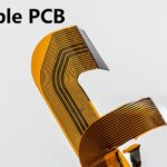
Flexible substrates use materials such as polyimide and are suitable for applications requiring bending, lightweight construction, or compact three-dimensional packaging.
Flexible IC Substrate Materials can provide useful mechanical flexibility while maintaining reliable electrical connections in space-constrained electronic products.
Ceramic IC Substrates
Ceramic substrates are commonly manufactured using materials such as aluminum oxide (Al₂O₃), aluminum nitride (AlN), and silicon carbide (SiC).
They provide excellent thermal stability, low CTE, high-temperature resistance, and strong thermal conductivity. Ceramic substrates are therefore suitable for high-power, high-temperature, RF, automotive, and other demanding applications.
Three Major IC Substrate Manufacturing Technologies
The selection of IC Substrate Manufacturing technology has a direct impact on line width, spacing, yield, production efficiency, and manufacturing cost.
The three major technologies are:
- Subtractive Process (SP)
- Additive Process (AP)
- Modified Semi-Additive Process (MSAP)
Subtractive Process (SP)
The subtractive process is conceptually similar to conventional PCB fabrication.
A copper layer is laminated onto the substrate, followed by dry-film application and photolithography. The unwanted copper is then removed through etching, leaving the required circuit pattern.
The achievable line width and spacing depend heavily on copper thickness, photoresist resolution, etching control, and equipment capability.
The subtractive process is relatively mature and cost-effective, but its ability to produce extremely fine features is limited by the etching process.
Additive Process (AP)
In the additive process, copper is selectively deposited onto the substrate rather than starting with a thick copper layer and removing the unwanted material.
A thin conductive seed layer is formed first. Photolithography defines the circuit pattern, after which copper is chemically or electrolytically deposited onto the required areas.
Because unnecessary copper removal is minimized, additive processing can achieve extremely fine circuit geometries.
However, AP requires sophisticated equipment and strict process control, making it more expensive than conventional subtractive processing.
Modified Semi-Additive Process (MSAP)
MSAP combines concepts from subtractive and additive manufacturing.
A thin copper layer is initially formed on the substrate. A photoresist is then applied to define the circuit pattern, and copper is plated selectively in the exposed areas.
After plating, the photoresist is removed and the original seed copper is etched away.
The thin starting copper layer reduces the amount of copper that needs to be etched, allowing MSAP to achieve finer line widths and spaces than conventional subtractive processing.
MSAP offers a practical balance between manufacturing precision, production efficiency, yield, and cost. It has therefore become an important technology for high-density IC substrate production.
IC Substrate Manufacturing Process
The IC Substrate Manufacturing process involves multiple precision-controlled steps.
1. Copper Pattern Formation
The required circuit pattern is transferred onto the substrate through photolithography and related imaging processes.
Copper is then plated to achieve the required conductor thickness and geometry. Precise control of plating uniformity is essential because variations in copper thickness can affect electrical performance and dimensional accuracy.
2. Microvia Formation
Microvias provide vertical electrical connections between different substrate layers.
Depending on the substrate structure, laser drilling is commonly used to create very small via structures. The hole diameter, depth, landing pad, and plating quality must all be tightly controlled.
3. Dielectric and Layer Formation
Multilayer IC substrates are built by repeatedly forming dielectric and copper layers.
The thickness and dielectric properties of each layer influence impedance, capacitance, signal propagation, and thermal behavior. Proper registration between layers is also critical for achieving reliable fine-pitch connections.
4. Solder Mask and Protective Layers
A solder mask or other protective layer may be applied to selected areas of the substrate.
The process must maintain precise openings around pads and connection areas while protecting conductive features from contamination and unintended solder bridging.
5. Surface Finish
The surface finish protects exposed copper and provides a reliable interface for semiconductor assembly and soldering.
Common finishes include:
- ENIG
- ENEPIG
- Electroless nickel
- Gold-based finishes
ENEPIG is particularly useful for applications requiring excellent surface uniformity, wire-bond compatibility, corrosion resistance, and reliable solderability.
6. Electrical and Reliability Testing
The final substrate undergoes electrical inspection and quality testing.
Depending on the product requirements, testing may include:
- Automated optical inspection (AOI)
- Electrical continuity and isolation testing
- Dimensional inspection
- Surface inspection
- Microvia quality inspection
- Solderability testing
- Thermal cycling and reliability testing
Testing helps identify open circuits, short circuits, dimensional deviations, plating defects, and other potential reliability issues before the substrate is assembled with the semiconductor device.
IC Substrate PCB Design Considerations
Designing an IC Substrate PCB requires much tighter control than designing a conventional PCB. Material selection, layer structure, routing density, pad geometry, thermal management, and manufacturing capability must all be considered at the beginning of the design process.
Material Selection
The dielectric material affects dielectric constant, dielectric loss, CTE, moisture absorption, thermal resistance, and mechanical stability.
For high-speed applications, low-loss materials may be required to minimize insertion loss and maintain signal integrity.
Fine-Line Routing
Advanced IC packages require extremely fine traces and spaces.
Designers must ensure that the selected geometry is compatible with the manufacturer’s actual process capability. Trace width, spacing, copper thickness, pad dimensions, and etching compensation should be considered together rather than independently.
Impedance Control
High-speed interfaces require controlled impedance.
The impedance depends on trace width, copper thickness, dielectric thickness, dielectric constant, reference-plane configuration, and conductor geometry.
Therefore, the substrate stackup must be designed together with the target electrical requirements.
Thermal Management
High-performance processors and GPUs can generate substantial heat.
The substrate design should consider thermal vias, copper distribution, heat spreaders, package construction, and the thermal path from the semiconductor die to the system-level PCB.
CTE Matching
The CTE difference between the semiconductor die, substrate, solder joints, and PCB can generate mechanical stress during temperature changes.
Appropriate material selection and package architecture can reduce this stress and improve long-term reliability.
Surface Finish
The surface finish must be compatible with the intended assembly technology.
ENIG and ENEPIG are frequently considered for advanced substrate applications because they provide controlled surface properties and good solderability.
Applications of IC Substrate PCBs
The demand for IC Substrate PCB technology continues to increase as electronic devices become smaller and semiconductor integration becomes more advanced.
Typical applications include:
- Smartphones and tablets
- CPUs and GPUs
- Memory devices
- Networking equipment
- Telecommunications systems
- AI accelerators
- Automotive electronics
- Medical electronics
- Aerospace systems
- Industrial control equipment
- Gaming processors and graphics systems
- High-performance computing equipment
In these applications, the substrate must provide high-density interconnection while maintaining electrical, thermal, mechanical, and reliability performance.
IC Substrate PCB vs. Conventional PCB
Although both products use copper conductors and dielectric materials, their manufacturing requirements are significantly different.
| Feature | IC Substrate PCB | Conventional PCB |
|---|---|---|
| Circuit density | Extremely high | Low to high |
| Trace/space | Very fine | Generally larger |
| Pad size | Very small | Larger |
| Dimensional tolerance | Extremely tight | Relatively relaxed |
| Microvias | Frequently required | Application dependent |
| Manufacturing precision | Very high | Moderate to high |
| Main purpose | Semiconductor packaging | System-level interconnection |
| Typical applications | CPUs, GPUs, memory, advanced ICs | Consumer, industrial, automotive, communication |
The fundamental difference is that an IC Substrate is designed to bridge the extremely fine-pitch connections of a semiconductor die with the comparatively larger interconnect structure of a PCB.
Why Choose Kingda for IC Substrate PCB Manufacturing?
As semiconductor packaging continues to evolve, choosing an experienced manufacturing partner is essential for achieving consistent quality and reliable production.
Kingda focuses on providing PCB and high-density interconnection solutions for demanding electronic applications. For IC substrate-related projects, important considerations include manufacturing precision, material selection, process control, inspection capability, and communication between design and manufacturing teams.
When evaluating an IC Substrate PCB supplier, customers should consider:
- Experience with high-density PCB and substrate technologies.
- Stable control of fine-line circuit fabrication.
- Appropriate material and surface-finish selection.
- Reliable microvia and multilayer process control.
- Comprehensive electrical and visual inspection.
- Flexible production support for prototype and volume requirements.
- Technical communication and engineering support.
- Consistent quality and dependable delivery.
Kingda can work with customers to evaluate substrate structures, material requirements, routing density, surface finishes, and manufacturing constraints so that the final design is better aligned with production capabilities.
Conclusion
An IC Substrate PCB is a critical component in advanced semiconductor packaging. It provides the electrical, mechanical, and thermal interface between the IC die and the system-level PCB while enabling extremely high-density interconnection.
As semiconductor devices continue to increase in integration and performance, technologies such as MSAP, ABF-based substrates, flip-chip packaging, microvias, and fine-line routing are becoming increasingly important.
Selecting suitable IC Substrate Materials, optimizing the stackup, controlling impedance and thermal performance, and choosing an appropriate IC Substrate Manufacturing process are all essential for achieving reliable and high-performance packages.
For applications involving processors, memory, communication devices, AI hardware, automotive electronics, and other advanced systems, Kingda can provide professional PCB manufacturing support tailored to the electrical, mechanical, thermal, and reliability requirements of the project.