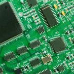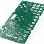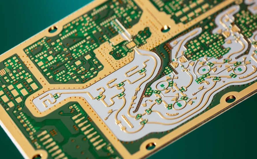
A Radar PCB is a specialized printed circuit board designed to support radar systems that transmit, receive, process, and analyze electromagnetic and radio-frequency (RF) signals. Radar technology is widely used to detect objects, determine their distance and position, track movement, and identify targets in environments where accurate sensing and reliable signal processing are essential.
Unlike conventional circuit boards, a Radar Circuit Board must handle high-frequency signals while maintaining controlled impedance, low signal loss, low noise, and excellent signal integrity. It typically integrates RF circuits, antenna interfaces, power management, signal-processing circuits, and communication interfaces into a compact structure.
Because radar systems often operate at demanding frequencies, the PCB material, stackup, trace geometry, grounding, via structure, and manufacturing tolerances all have a direct impact on system performance. Therefore, radar PCB design and manufacturing require careful coordination between electrical design and PCB fabrication.
Basic Components of a Radar PCB
A radar system operates by transmitting electromagnetic waves and analyzing the signals reflected from objects. The reflected signal contains information that can be used to determine characteristics such as distance, direction, movement, and relative velocity.
The PCB serves as the electrical foundation connecting the major functional blocks of the radar system. A typical radar PCB may contain the following components:
- Transmitter: Generates and amplifies the RF signal that is transmitted toward the target.
- Receiver: Captures reflected signals and processes weak RF signals returned from the target.
- Antenna interface: Connects the RF circuitry to the antenna for transmitting and receiving electromagnetic waves.
- Duplexer or RF switch: Allows the antenna to share transmitting and receiving functions in systems that use a common antenna path.
- Waveguide or RF transmission structure: Provides a controlled path for high-frequency signal transmission where required by the system architecture.
- Signal detection and processing circuit: Analyzes received signals and extracts useful information such as target distance, direction, speed, or movement.
Modern radar systems may also integrate mixers, low-noise amplifiers (LNAs), power amplifiers (PAs), filters, oscillators, frequency synthesizers, analog-to-digital converters, processors, memory, and communication interfaces.
Key Characteristics of Radar PCB
A Radar PCB must meet significantly higher electrical and manufacturing requirements than many conventional PCBs. The most important characteristics include:
High-Frequency Performance
Radar systems rely on high-frequency electromagnetic signals. As operating frequency increases, transmission losses, dielectric properties, conductor surface roughness, and parasitic effects become increasingly important.
A suitable High-Frequency PCB material should provide stable dielectric properties, low dissipation factor, and predictable electrical performance across the intended frequency range.
Controlled Impedance
Impedance control is essential for maintaining signal integrity in RF transmission paths. The PCB stackup, dielectric thickness, copper thickness, trace width, and material characteristics must be carefully controlled to achieve the required impedance.
Improper impedance can cause signal reflections, insertion loss, and distortion, reducing radar detection accuracy.
Low Signal Loss and Noise
Radar receivers may need to detect very weak reflected signals. Excessive insertion loss, electromagnetic interference, crosstalk, or power-supply noise can reduce receiver sensitivity.
PCB layout should therefore provide short RF paths, appropriate grounding structures, adequate isolation between functional blocks, and carefully designed power distribution.
Compact and High-Density Construction
Radar electronics are often integrated into compact devices. A high-density layout allows RF, digital, analog, power, and control circuits to occupy limited board space.
HDI technology, microvias, fine-pitch components, and multilayer construction can be considered when the design requires higher routing density.
Mechanical and Environmental Reliability
Radar equipment may operate in vehicles, industrial environments, outdoor equipment, aerospace systems, or other demanding conditions. The PCB should therefore provide appropriate mechanical strength and resistance to temperature variation, humidity, vibration, and other environmental stresses.
Types of Radar PCB
Different radar architectures require different PCB configurations. Common radar applications include the following types:
| Radar PCB Type | Description |
|---|---|
| Monopulse Radar PCB | Supports radar architectures that determine target direction by comparing signals received through multiple channels. |
| Doppler Radar PCB | Designed for systems that measure target motion and velocity by analyzing frequency shifts in reflected signals. |
| Weather Radar PCB | Used in weather-monitoring systems to detect and analyze precipitation, storm activity, and atmospheric conditions. |
| Passive Radar PCB | Supports radar systems that use existing external electromagnetic transmissions rather than relying entirely on a dedicated transmitter. |
| Pulse Radar PCB | Used in systems that transmit high-frequency pulses and analyze their reflections to determine target characteristics. |
| Automotive Radar PCB | Designed for vehicle sensing applications such as object detection, collision avoidance, adaptive cruise control, and blind-spot monitoring. |
The actual PCB architecture depends on the radar frequency, antenna configuration, required detection range, signal-processing method, power level, mechanical constraints, and environmental requirements.
Applications of Radar PCB
Radar technology is used across many industries because it can detect objects and movement without requiring direct visual contact.
1. Military and Defense Applications
Radar PCBs are widely used in defense systems for target detection, tracking, navigation, surveillance, and situational awareness. They may support systems used for monitoring aircraft, ships, vehicles, terrain, and other targets.
Because defense equipment can operate under severe environmental and electrical conditions, the PCB must provide stable RF performance and high reliability.
2. Automotive Applications
Automotive radar has become an important sensing technology for modern vehicles. A Radar Sensor PCB can support functions such as:
- Adaptive cruise control
- Automatic emergency braking
- Blind-spot detection
- Lane-change assistance
- Forward collision warning
- Parking assistance
- Object and pedestrian detection
Automotive radar commonly requires compact board structures, controlled RF characteristics, strong vibration resistance, and stable operation across a wide temperature range.
3. Aerospace and Space Applications
Radar electronics can be used in aircraft, spacecraft, satellites, and other aerospace systems for navigation, object detection, terrain observation, and scientific measurement.
In these applications, PCB design must consider weight, size, thermal management, vibration, reliability, and environmental conditions.
4. Weather Monitoring
Weather radar systems use electromagnetic waves to detect precipitation and analyze atmospheric conditions. Radar PCBs provide the RF transmission, reception, signal processing, and control functions required by these systems.
High signal stability and low-noise performance are especially important when detecting weak reflected signals over long distances.
5. Security and Smart Sensing
Radar sensors are increasingly used in security and smart-building applications. Radar-based sensing can detect movement and determine the presence or location of objects without relying entirely on optical cameras.
Applications include intrusion detection, automatic door control, occupancy detection, smart lighting, and other intelligent sensing systems.
6. Industrial Applications
Industrial radar systems can be used for level measurement, object detection, process monitoring, motion detection, and automation.
In industrial environments, the PCB may need to withstand electromagnetic interference, temperature changes, vibration, dust, humidity, and continuous operation.
Radar PCB Design Process
The design of a radar circuit board depends heavily on the radar architecture and its operating frequency. RF circuits, digital processing circuits, power circuits, and control circuits may have very different electrical requirements.
A successful PCB Design process should therefore consider electrical performance, mechanical requirements, manufacturing capability, and system-level requirements from the beginning.
1. Define System Requirements
Before creating the PCB schematic, engineers should determine key parameters such as:
- Operating frequency
- Required bandwidth
- Transmit power
- Receiver sensitivity
- Target detection range
- Antenna configuration
- Required impedance
- Number of signal layers
- Power requirements
- Environmental conditions
- Board dimensions
These requirements establish the foundation for the PCB stackup and component selection.
2. Develop the Schematic
The schematic should include all major functional blocks of the Radar System, including the transmitter, receiver, RF front end, signal-processing circuitry, power supply, control circuitry, and communication interfaces.
Separating different functional blocks during schematic development makes it easier to evaluate signal paths and identify potential interference sources.
3. Design the RF Section
The RF section is one of the most critical parts of a radar PCB. Components such as amplifiers, filters, mixers, oscillators, RF switches, and frequency synthesizers should be positioned according to the signal flow.
RF traces should generally be kept short and designed with controlled impedance. Unnecessary bends, discontinuities, stubs, and abrupt changes in transmission geometry should be minimized.
4. Design the Antenna Interface
The antenna interface must match the requirements of the radar system. Engineers should consider antenna impedance, frequency response, gain, radiation pattern, connector structure, and transmission-line characteristics.
For integrated antennas, PCB material and board geometry can directly affect antenna performance, so electromagnetic simulation may be necessary during development.
5. Plan the PCB Stackup
A multilayer structure can provide separate routing, grounding, power, and RF layers. A properly designed stackup helps reduce electromagnetic coupling and provides stable reference planes for high-speed and RF signals.
The dielectric thickness between the RF trace and reference plane must be carefully controlled because it directly influences transmission-line impedance.
6. Control Signal Integrity
Signal integrity is particularly important for radar systems because small signal distortions can affect detection and measurement accuracy.
Designers should evaluate:
- Controlled impedance
- Insertion loss
- Return loss
- Crosstalk
- Ground integrity
- Power-supply noise
- Electromagnetic interference
- Via discontinuities
- Trace length and routing geometry
Simulation and verification can help identify potential signal-integrity problems before production.
7. Improve Thermal Management
High-power RF components, power amplifiers, processors, and power-management devices can generate substantial heat.
Thermal vias, copper planes, heat spreaders, appropriate component placement, and suitable PCB materials can be used to improve heat dissipation. Thermal management should be considered together with electrical and mechanical design rather than treated as a final-stage adjustment.
8. Select Appropriate Materials
Material selection has a direct impact on RF performance. Depending on the operating frequency and performance requirements, radar PCBs may use high-frequency laminates or combinations of conventional and high-frequency materials.
Materials such as PTFE-based laminates, high-frequency hydrocarbon/ceramic materials, and other RF-oriented substrates may be considered depending on the design.
Material selection should take into account dielectric constant, dissipation factor, thermal stability, dimensional stability, copper adhesion, moisture absorption, and manufacturing compatibility.
Materials Used for Radar PCB
The substrate is particularly important in high-frequency applications because dielectric properties influence signal propagation.
PTFE-Based Materials
PTFE-based materials are widely used in high-frequency applications because of their low dielectric loss and favorable RF characteristics. They can be suitable for radar designs requiring low transmission loss.
However, PTFE materials may require specialized fabrication processes because of their mechanical and dimensional characteristics.
High-Frequency Laminates
High-frequency laminates are designed to provide stable electrical properties at elevated frequencies. They are suitable for RF transmission lines, antenna structures, filters, and other high-frequency circuits.
Hybrid PCB Materials
Some radar designs combine different laminate materials within the same stackup. This approach can balance RF performance, mechanical properties, thermal performance, and manufacturing cost.
The appropriate material should be selected according to the actual operating frequency, signal requirements, layer structure, environmental conditions, and manufacturing process.
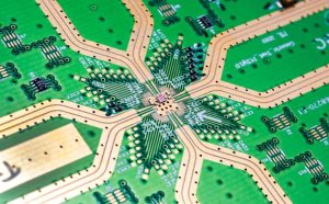
Important Radar PCB Manufacturing Considerations
Manufacturing precision is critical because even small dimensional variations can influence RF performance.
Key manufacturing considerations include:
- Controlled trace width and spacing
- Stable dielectric thickness
- Consistent copper thickness
- Accurate layer registration
- Reliable via structures
- Controlled surface roughness
- High-quality soldering
- Appropriate surface finish
- Reliable plated-through holes and microvias
- Comprehensive electrical testing
For high-frequency applications, PCB fabrication should be closely coordinated with the original design data. Manufacturing tolerances should be evaluated during the design stage to avoid unexpected impedance variations or signal loss.
Why Choose Kingda for Radar PCB Manufacturing?
Radar PCB manufacturing requires more than standard board fabrication. It requires careful control of materials, impedance, RF structures, layer alignment, and manufacturing consistency.
Kingda can provide PCB manufacturing and assembly solutions based on the specific requirements of radar and other high-frequency electronic applications.
Professional Manufacturing Support
Radar projects often involve complex RF structures and multilayer configurations. A professional manufacturing process helps maintain consistency between the PCB design and the final physical board.
Flexible Customization
Different radar systems operate at different frequencies and have different antenna, power, layer, size, and environmental requirements. Custom PCB manufacturing allows the board structure to be adapted to the specific application.
Quality-Focused Production
Because radar systems can be highly sensitive to electrical variations, quality control is essential throughout PCB manufacturing. Inspection and testing can help identify manufacturing defects that could affect RF performance and long-term reliability.
Support for High-Frequency PCB Requirements
For high-frequency applications, material selection, impedance control, copper geometry, stackup design, and RF routing all need to work together. These factors should be considered from design through manufacturing to achieve stable performance.
Cost and Production Efficiency
A suitable manufacturing strategy can help balance RF performance, board complexity, production volume, and project cost. Early communication between the PCB designer and manufacturer can also reduce manufacturing risks and unnecessary redesigns.

Radar PCB Design Best Practices
To achieve stable and reliable radar performance, designers should consider the following practices:
- Keep RF signal paths short and direct.
- Use controlled-impedance transmission lines for critical RF signals.
- Maintain continuous and low-impedance ground references.
- Separate RF, digital, analog, and high-power circuits appropriately.
- Minimize unnecessary vias and transmission-line discontinuities.
- Keep noisy power circuits away from sensitive receiver paths.
- Use appropriate shielding or grounding structures when necessary.
- Select PCB materials according to the actual operating frequency.
- Consider thermal performance during component placement and stackup design.
- Verify the design against the PCB manufacturer’s actual process capabilities.
Conclusion
A Radar PCB is a critical part of modern radar electronics and directly affects RF transmission, signal reception, processing accuracy, and overall system reliability. As radar technology moves toward higher frequencies, smaller form factors, greater detection accuracy, and more integrated architectures, PCB design and manufacturing requirements are becoming increasingly demanding.
A well-designed Radar Circuit Board should combine controlled impedance, low-loss materials, effective grounding, reliable thermal management, accurate manufacturing, and strong signal integrity. For automotive, industrial, aerospace, defense, weather monitoring, and smart-sensing applications, selecting an experienced PCB manufacturing partner can help ensure that the final board meets the electrical, mechanical, and environmental requirements of the radar system.
Kingda provides customized PCB manufacturing and assembly solutions to support demanding RF and high-frequency electronic applications, helping customers move from PCB design requirements to reliable production.