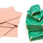
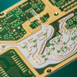
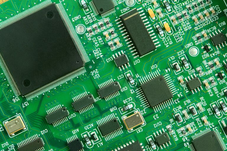
Surface Mount Technology (SMT) has fundamentally transformed modern electronics manufacturing by enabling electronic components to be mounted directly onto the surface of a printed circuit board (PCB). Compared with traditional Through-Hole Technology (THT), SMT supports smaller component packages, higher assembly density, faster automated production, and improved suitability for compact and high-performance electronic products.
Today, SMT assembly is widely used in computers, telecommunications equipment, automotive electronics, medical devices, industrial automation, consumer electronics, aerospace systems, and other advanced applications. The continuous development of smaller component packages, high-speed placement equipment, intelligent inspection systems, and advanced PCB technologies has further strengthened SMT’s position as a core technology in modern PCB assembly.
As an experienced PCB manufacturer and PCB assembly service provider, Kingda provides integrated PCB prototype manufacturing, quick-turn PCB prototyping, SMT assembly, THT assembly, inspection, testing, and PCBA manufacturing solutions. Our capabilities support customers from initial design verification and prototype production through small-batch manufacturing and volume production.
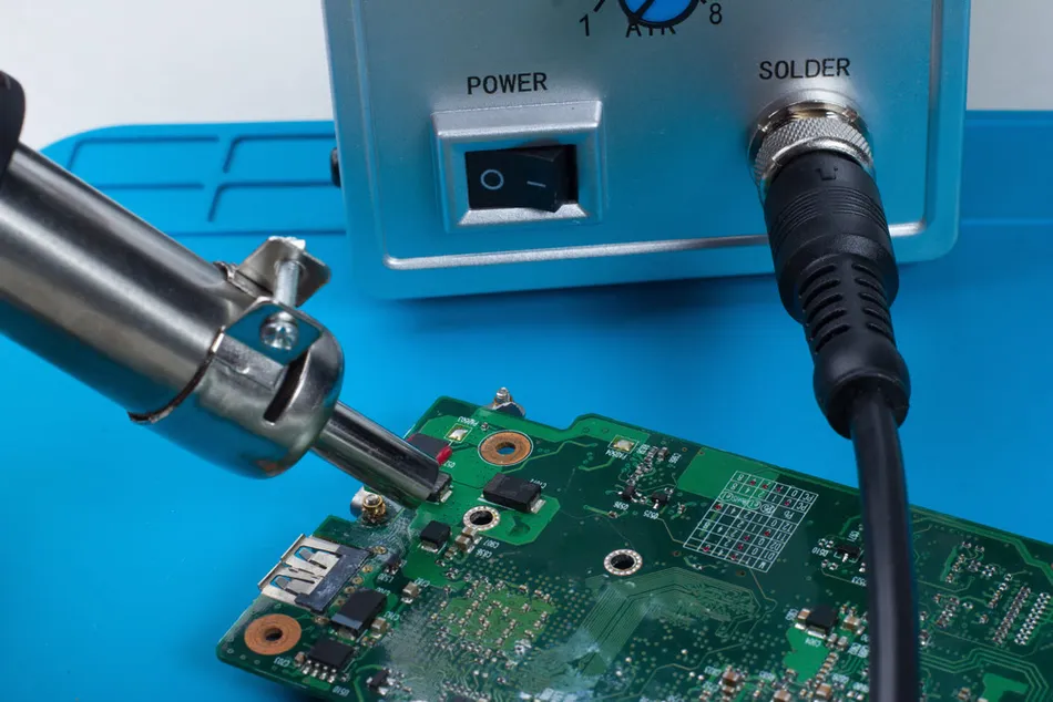
This guide explains the development of Surface Mount Technology, its core advantages, major process technologies, component packaging trends, ESD protection requirements, key SMT manufacturing parameters, and the role of intelligent production systems.
What Is Surface Mount Technology?
Surface Mount Technology (SMT) is an electronic assembly technology in which components are mounted directly onto solder pads on the surface of a PCB.
The components used in SMT are known as Surface Mount Devices (SMDs). Unlike traditional through-hole components, SMDs typically use short leads, terminals, or metal contacts that are soldered directly to PCB pads.
A typical SMT assembly process includes:
PCB Loading → Solder Paste Printing → SPI → SMD Placement → Reflow Soldering → AOI → X-Ray Inspection → Electrical Testing → Final Inspection
Depending on the product, additional processes such as cleaning, conformal coating, selective soldering, functional testing, and burn-in testing may also be required.
The combination of automated equipment and controlled manufacturing parameters enables SMT to achieve high throughput while maintaining consistent assembly quality.
Evolution and Technical Background of SMT
Why SMT Was Developed
The continuous development of electronic products has created three major requirements for PCB assembly:
- Higher component density
- Higher manufacturing efficiency
- Greater standardization and automation
Traditional through-hole assembly requires component leads to pass through drilled holes. Although THT provides excellent mechanical strength, the required holes consume valuable PCB space and limit component density.
SMT technology addresses these limitations by placing components directly onto the PCB surface. This allows manufacturers to reduce component size, increase circuit density, use both sides of the PCB, and automate much of the assembly process.
Development of SMT Technology
The development of SMT can generally be divided into several stages.
Early Development
SMT technology began emerging during the 1960s and 1970s. Early applications were concentrated in hybrid circuits and products requiring relatively compact electronic assemblies.
Rapid Development
During the 1980s, SMT equipment, components, soldering technologies, and manufacturing processes developed rapidly. Automated component placement became increasingly practical for commercial electronics manufacturing.
Mainstream Adoption
During the 1990s, SMT became a mainstream assembly method across consumer electronics, computers, telecommunications, and industrial electronics.
Modern SMT Manufacturing
In the 21st century, SMT has continued evolving toward:
- Smaller component packages
- Higher I/O density
- Faster placement
- Better placement accuracy
- Advanced soldering materials
- Automated inspection
- Digital manufacturing
- Full production traceability
Modern SMT PCB assembly is no longer simply a component placement process. It is an integrated manufacturing system combining engineering data, automation, process control, inspection, testing, and production analytics.
Core Advantages of SMT Technology
1. High-Density PCB Assembly
One of the most important advantages of SMT assembly is its ability to support high component density.
Because SMD components do not require leads to pass through drilled holes, designers can place components much closer together. Components can also be mounted on both sides of the PCB.
This makes SMT particularly suitable for:
- Smartphones
- Wearable electronics
- IoT devices
- Communication modules
- Portable medical devices
- High-density computing systems
2. High-Speed Automated Manufacturing
SMT is highly compatible with automated production.
Modern SMT lines can integrate:
- Automatic solder paste printers
- 3D SPI systems
- High-speed pick-and-place machines
- Reflow ovens
- 3D AOI systems
- X-ray inspection systems
- Automated testing equipment
Automation reduces manual handling and improves manufacturing consistency, repeatability, and production throughput.
3. Improved High-Frequency Performance
SMD components generally have much shorter electrical paths than conventional through-hole components.
Shorter connections can reduce parasitic inductance and capacitance, which is beneficial for:
- High-frequency circuits
- RF systems
- High-speed digital electronics
- Communication equipment
- Signal integrity
- EMI control
For advanced electronic products, proper SMT PCB design can therefore contribute to improved electrical performance.
4. Smaller and Lighter Products
SMT supports the continuous miniaturization of electronic products.
Smaller components and higher PCB density allow designers to reduce the overall size and weight of electronic assemblies without necessarily reducing functionality.
5. Cost Efficiency in Volume Production
Although SMT equipment requires considerable initial investment, automated production can significantly reduce labor requirements and improve throughput.
For medium- and high-volume production, automated SMT manufacturing can provide strong cost advantages through:
- Higher production speed
- Reduced manual labor
- Efficient material handling
- Lower assembly time
- Better process repeatability
6. Excellent Design Flexibility
SMT supports complex PCB layouts and high-density multilayer designs.
It is compatible with technologies such as:
- HDI PCB
- Flexible PCB
- Rigid-flex PCB
- High-density multilayer PCB
- Fine-pitch PCB
- High-speed PCB
Key Technological Trends in SMT
Component Packaging Innovation
One of the most important trends in SMT is the continuous evolution of component packaging.
Modern packaging technologies increasingly focus on:
- Smaller package dimensions
- Higher pin counts
- Improved thermal performance
- Higher electrical performance
- Greater integration
Examples include:
- Multi-Chip Modules (MCM)
- System-in-Package (SiP)
- System-on-Chip (SoC)
- Chip-scale packages
- Fine-pitch packages
- Advanced BGA packages
- High-density semiconductor packages
These technologies allow more functionality to be integrated into smaller spaces.
SMT Equipment Development
Modern SMT production equipment is increasingly focused on speed, precision, flexibility, and intelligent manufacturing.
High-Speed Placement
Advanced placement machines use multiple placement heads and optimized feeder configurations to increase throughput.
Intelligent Vision Systems
High-resolution vision systems verify component orientation and position before placement.
Flexible Production Lines
Modular SMT equipment allows manufacturers to adjust production lines for different board sizes, component types, and production volumes.
Intelligent Manufacturing
Modern SMT factories increasingly integrate MES systems, machine data collection, process monitoring, and production traceability.
These technologies allow manufacturers to monitor production parameters in real time and quickly identify process deviations.
PCB Technology Trends Supporting SMT
The development of SMT assembly is closely connected to advances in PCB manufacturing.
Modern PCB technologies increasingly focus on:
Fine-Line PCB Manufacturing
Fine-line and fine-spacing technologies enable high-density circuit layouts.
HDI PCB
High-Density Interconnect (HDI) PCB technology uses microvias, fine lines, and high-density routing to support advanced component packages and compact electronic designs.
Multilayer PCB
High-layer-count PCBs provide additional routing capacity for complex electronic systems.
Flexible PCB
Flexible circuits enable electronic products to achieve smaller form factors and more flexible mechanical structures.
Rigid-Flex PCB
Rigid-flex boards combine rigid and flexible sections to reduce connectors and improve system integration.
Advanced PCB Materials
High-frequency, high-Tg, low-loss, and thermally enhanced materials are increasingly used in demanding electronic applications.
Core SMT Assembly Processes
A reliable SMT assembly process depends on precise control of several key manufacturing stages.
1. Solder Paste Printing
Solder paste printing is the first major process in SMT production.
A precision stainless-steel stencil is aligned with the PCB, and a squeegee forces solder paste through stencil apertures onto the designated PCB pads.
Important process parameters include:
- Stencil thickness
- Aperture geometry
- Squeegee speed
- Squeegee pressure
- Printing angle
- PCB support
- Solder paste condition
- Environmental conditions
For fine-pitch components, stencil aperture design becomes particularly important.
A poorly designed stencil can cause insufficient solder, bridging, solder balling, or inconsistent solder deposition.
2. Solder Paste Inspection
After printing, Solder Paste Inspection (SPI) verifies the quality of solder paste deposition.
Modern 3D SPI systems can measure:
- Paste volume
- Paste height
- Paste area
- Paste position
- Printing offset
SPI is valuable because it detects printing problems before components are placed and reflowed.
3. Component Placement
The pick-and-place process is the central placement stage of SMT assembly.
Automated placement machines pick components from reels, trays, or other feeders and place them onto the corresponding solder paste deposits.
Key process factors include:
- Placement accuracy
- Feeder calibration
- Nozzle selection
- Component recognition
- Component polarity
- Placement force
- Vision alignment
For high-density assemblies, precise placement is essential to avoid solder bridges, misalignment, and other assembly defects.
4. Reflow Soldering
After component placement, the PCB passes through a reflow soldering oven.
The board is gradually heated according to a carefully controlled temperature profile.
A typical reflow process includes:
Preheating → Soaking → Reflow → Cooling
During the reflow stage, solder melts and forms metallurgical connections between SMD terminals and PCB pads.
The temperature profile must be optimized according to:
- Solder alloy
- PCB thickness
- Component thermal mass
- Component specifications
- PCB material
- Assembly requirements
Incorrect reflow parameters can cause cold solder joints, component damage, tombstoning, voiding, or solder bridging.
SMT ESD Protection and Management
Electrostatic Discharge (ESD) is an important concern in electronic assembly.
A static discharge may cause immediate component failure or latent damage that becomes apparent only after the product has been deployed.
Common ESD Protection Measures
Personnel Protection
Production personnel may use:
- ESD wrist straps
- ESD footwear
- ESD garments
- Grounding systems
ESD-Safe Work Environment
Manufacturing facilities can use:
- ESD-safe workstations
- Conductive flooring
- Grounded equipment
- ESD-safe storage systems
Process Control
An effective ESD management system should include:
- Regular grounding checks
- Personnel compliance procedures
- ESD monitoring
- Proper component storage
- Controlled material handling
ESD protection is particularly important when assembling sensitive semiconductor devices, microcontrollers, memory devices, sensors, and other static-sensitive components.
Three Critical SMT Process Technologies
1. Solder Paste Printing Technology
Solder paste printing directly affects solder joint quality.
Typical process considerations include:
- Automatic vision alignment
- Appropriate stencil thickness
- Optimized aperture ratios
- Controlled squeegee speed
- Controlled printing pressure
- Proper solder paste storage
- Stable production temperature and humidity
For fine-pitch PCB assembly, stencil design and paste-release performance become increasingly important.
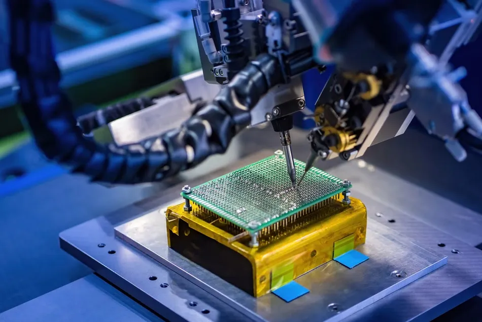
2. Precision Component Placement
Component placement accuracy directly influences final assembly quality.
Modern placement systems use vision recognition to identify:
- Component position
- Orientation
- Polarity
- Package characteristics
Regular feeder calibration, nozzle maintenance, and vision-system calibration are essential for stable placement performance.
3. Reflow Soldering
Reflow soldering determines whether the solder paste successfully forms reliable electrical and mechanical joints.
Engineers monitor:
- Ramp rate
- Soak temperature
- Peak temperature
- Time above liquidus
- Cooling rate
- Oven atmosphere
- Conveyor speed
The appropriate profile should always be established according to the specific solder paste and assembly requirements rather than relying on a universal temperature curve.
Common SMT Assembly Defects
Understanding common defects helps manufacturers improve SMT PCB assembly quality.
Tombstoning
Tombstoning occurs when one end of a small passive component rises from the PCB pad during reflow.
Potential causes include:
- Uneven solder paste deposition
- Pad design imbalance
- Uneven heating
- Component placement offset
Solder Bridging
Solder bridging occurs when molten solder connects adjacent pads or terminals.
Possible causes include:
- Excessive solder paste
- Incorrect stencil apertures
- Excessive component density
- Poor printing alignment
Insufficient Solder
Insufficient solder may result from inadequate paste volume, poor stencil design, or printing process instability.
Component Misalignment
Component offset can result from incorrect placement coordinates, feeder problems, vision errors, or excessive movement before reflow.
Cold Solder Joints
Cold joints can occur when the solder does not reach an appropriate temperature or remains above liquidus for insufficient time.
Process control and temperature-profile verification are essential to prevent these defects.
SMT Inspection and Quality Control
High-quality SMT assembly services require inspection throughout the manufacturing process.
SPI Inspection
SPI checks solder paste deposition before component placement.
AOI Inspection
Automated Optical Inspection (AOI) can detect:
- Missing components
- Incorrect orientation
- Component displacement
- Solder bridges
- Insufficient solder
- Lead alignment problems
X-Ray Inspection
X-ray inspection is particularly useful for components whose solder joints cannot be visually inspected.
Typical applications include:
- BGA
- QFN
- LGA
- Bottom-terminated components
X-ray can help identify hidden solder defects such as voids, incomplete joints, and internal connection problems.
Electrical Testing
Depending on the product, manufacturers may perform:
- ICT
- Flying Probe Testing
- Functional Testing
- Power-up testing
- Communication testing
Combining process inspection and electrical testing provides more comprehensive quality assurance.
Intelligent SMT Manufacturing and MES
The development of Industry 4.0 is changing the way SMT manufacturing is managed.
Modern production lines can connect manufacturing equipment with Manufacturing Execution Systems (MES) to monitor production data in real time.
Important production data may include:
- PCB identification
- Component information
- Placement data
- Solder paste printing results
- SPI data
- AOI results
- Reflow temperature profiles
- X-ray inspection results
- Electrical test results
This approach improves:
- Process traceability
- Production visibility
- Quality management
- Defect analysis
- Process optimization
- Manufacturing consistency
For high-reliability products, complete production traceability can also support quality investigations and long-term product management.
SMT Assembly Applications
SMT technology is used across almost every major electronics sector.
Consumer Electronics
Smartphones, tablets, wearable devices, smart home products, and portable electronics rely heavily on SMT.
Telecommunications
Routers, network equipment, wireless modules, optical communication equipment, and communication infrastructure use high-density SMT assemblies.
Automotive Electronics
SMT is widely used in:
- ECUs
- ADAS systems
- Battery management systems
- Infotainment
- Automotive sensors
- Power electronics
Medical Electronics
Medical monitoring devices, diagnostic equipment, laboratory instruments, and medical control systems require precise and reliable PCB assemblies.
Industrial Automation
Industrial controllers, sensors, motor control systems, PLCs, instrumentation, and automation equipment commonly combine SMT and THT.
Aerospace and Defense
Aerospace electronics require strict reliability and manufacturing controls. SMT provides high-density assembly, while THT can be used for mechanically demanding components.
SMT vs. THT Assembly
SMT and THT are not necessarily competing technologies. Many modern electronic products use both.
| Feature | SMT Assembly | THT Assembly |
|---|---|---|
| Component Density | Very High | Lower |
| Assembly Speed | Very High | Moderate |
| Automation | Excellent | Good |
| Board Size | Compact | Generally Larger |
| Fine-Pitch Components | Excellent | Limited |
| Mechanical Strength | Good | Excellent |
| High-Power Components | Good | Excellent |
| Repairability | More Difficult | Easier |
| Double-Sided Assembly | Excellent | More Limited |
| Typical Applications | Consumer, telecom, medical, computing | Power, industrial, automotive, aerospace |
For many complex products, mixed-technology PCB assembly provides the best balance between miniaturization, electrical performance, mechanical strength, and manufacturing efficiency.
Why Choose Kingda for SMT PCB Assembly?
As an experienced PCB manufacturer and PCB assembly service provider, Kingda provides integrated solutions covering the complete electronic manufacturing process.
PCB Prototype Manufacturing
Kingda provides PCB prototype manufacturing and quick-turn PCB prototyping to help customers validate circuit designs before entering volume production.
Prototype services can help engineers verify:
- PCB layout
- Component selection
- Assembly feasibility
- Electrical performance
- Thermal considerations
- Manufacturing processes
DFM Engineering Support
Kingda provides engineering support to identify potential manufacturing and assembly issues before production.
DFM/DFA review can evaluate:
- Component spacing
- Pad design
- PCB tolerances
- Assembly clearances
- Component availability
- Fine-pitch requirements
- Soldering considerations
Early engineering review can reduce unnecessary design iterations and improve production readiness.
Integrated PCB and PCBA Manufacturing
Kingda combines PCB fabrication and PCB assembly capabilities to simplify the manufacturing process.
Customers can obtain:
PCB Manufacturing → Component Sourcing → SMT Assembly → THT Assembly → Inspection → Testing → PCBA Production
from a coordinated manufacturing partner.
SMT and THT Assembly
Kingda supports both SMT assembly and THT assembly, making it possible to manufacture mixed-technology PCBAs containing fine-pitch SMDs, connectors, transformers, relays, power components, and other specialized devices.
Quality Inspection and Testing
Kingda can integrate appropriate quality-control processes according to project requirements, including:
- SPI
- AOI
- X-ray inspection
- Visual inspection
- ICT
- Flying Probe Testing
- Functional Testing
- Final inspection
These processes help ensure that PCBAs meet defined electrical, mechanical, and manufacturing requirements.
From Prototype to Volume Production
Kingda supports customers throughout different stages of product development:
PCB Prototype → Quick-Turn Prototype → Engineering Validation → Small-Batch Production → Volume Manufacturing
This enables a smoother transition from product development to commercial production while maintaining manufacturing consistency.
Conclusion
Surface Mount Technology (SMT) has become a fundamental technology in modern PCB assembly, enabling manufacturers to achieve high component density, compact product designs, high-speed automated production, and excellent suitability for advanced electronic systems.
The core SMT manufacturing process includes solder paste printing, SPI, SMD componenlacement, reflow soldering, AOI, X-ray inspection, and electrical testing. Maintaining stable process parameters at every stage is essential for achieving reliable solder joints and consistent PCBA quality.
At the same time, SMT continues to evolve through smaller component packages, advanced PCB technologies, intelligent manufacturing systems, high-precision inspection equipment, and improved process traceability.
As an experienced PCB manufacturer and PCB assembly service provider, Kingda provides professional PCB prototype manufacturing, quick-turn PCB prototyping, SMT assembly, THT assembly, inspection, testing, and PCBA manufacturing solutions. From initial design verification to small-batch and volume production, Kingda helps customers improve manufacturability, maintain consistent quality, and accelerate the transition from prototype to reliable electronic products.