What Is a PCB Made Of? PCB Design, PCB Manufacturing & Circuit Board Materials Guide
The rapid advancement of technology is driving the printed circuit board (PCB) industry to continuously adapt to new engineering requirements. Major developments in industrial automation, advanced driver assistance systems (ADAS), wireless communication, remote tracking, artificial intelligence, and high-performance computing are creating demand for PCBs with higher reliability, greater electrical performance, better thermal management, and more compact form factors.
But what exactly is a PCB made of?
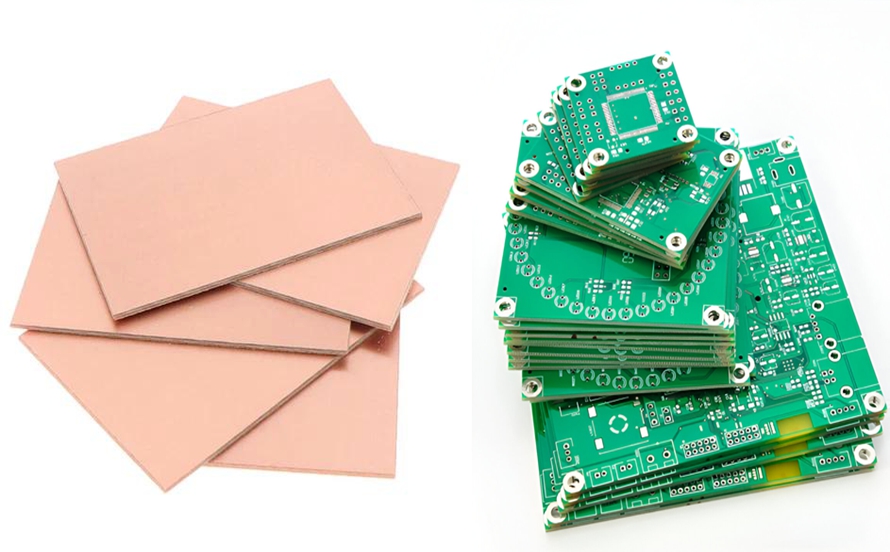
A printed circuit board is not simply a piece of fiberglass with copper attached to it. A typical PCB is an engineered combination of dielectric materials, copper conductors, resin systems, solder mask, surface finishes, and identification markings. In multilayer boards, these materials are carefully arranged into a controlled stack-up to provide mechanical strength, electrical insulation, signal routing, power distribution, and thermal performance.
Understanding the materials used in a PCB is therefore essential for engineers, designers, procurement teams, and manufacturers. The right material selection directly affects PCB Design, PCB Manufacturing, signal integrity, thermal reliability, mechanical stability, and the service life of the finished product.
What Materials Are Used to Make a PCB?
The exact material composition of a PCB depends on its construction, application, performance requirements, and manufacturing process. However, most conventional rigid PCBs contain several fundamental material categories.
1. PCB Substrate
The substrate, commonly referred to as a laminate, provides the structural foundation of the circuit board.
For rigid PCBs, the substrate is typically made from a combination of woven glass fiber and resin. It provides mechanical strength, dimensional stability, electrical insulation, and controlled dielectric characteristics.
For flexible PCBs, materials such as polyimide are commonly used instead because flexibility and resistance to repeated bending are important.
The substrate therefore plays a fundamental role in PCB Design because its dielectric constant, dissipation factor, thickness, thermal expansion, and mechanical properties influence the overall board design.
2. Copper Foil
Copper is the primary conductive material used in PCBs.
During PCB fabrication, copper is patterned to create electrical pathways such as:
- Signal traces
- Component pads
- Copper pours
- Ground planes
- Power planes
- Via structures
Copper thickness is an important design parameter because it affects current-carrying capability, resistance, heat generation, impedance, and manufacturing requirements.
Standard copper weights are often specified in ounces per square foot, such as 0.5 oz, 1 oz, 2 oz, or heavier copper constructions. High-current applications may require significantly thicker copper.
In high-speed PCB Design, trace geometry and copper characteristics also influence impedance control and signal integrity.
3. Dielectric Materials: Core and Prepreg
In multilayer PCBs, dielectric materials separate conductive copper layers and provide electrical insulation.
Two major laminate components are the core and prepreg.
A core is a cured laminate structure consisting of dielectric material with copper foil bonded to one or both sides. FR-4 is one of the most widely used core materials.
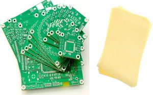
Prepreg, short for “pre-impregnated material,” generally consists of woven glass fiber impregnated with partially cured resin. During lamination, heat and pressure cause the resin to flow and cure, bonding the individual PCB layers into a solid multilayer structure.
The thickness and dielectric properties of core and prepreg materials are critical to controlled-impedance designs. Engineers must carefully define the stack-up to achieve the required electrical spacing and signal performance.
4. Solder Mask
Solder mask is the protective polymer coating applied over most of the outer copper surface.
Its primary functions include:
- Protecting copper from environmental exposure
- Reducing the risk of accidental solder bridges
- Providing electrical insulation between exposed conductive areas
- Improving PCB durability
- Defining the areas where solder can be applied
Green is the most recognizable solder mask color, but black, blue, red, white, yellow, and other colors are also available.
During PCB Manufacturing, solder mask application must be accurately controlled because excessive or insufficient coverage can affect solderability, insulation, inspection, and appearance.
5. Silkscreen
Silkscreen is the identification and marking layer printed on the PCB surface.
It may contain:
- Component reference designators
- Polarity indicators
- Pin-1 markings
- Connector labels
- Logos
- Manufacturing codes
- Revision information
- Traceability information
Silkscreen improves assembly efficiency by helping operators and automated equipment identify components and locations.
Although silkscreen does not normally perform an electrical function, accurate markings can significantly improve PCB assembly, inspection, maintenance, and product traceability.
6. Surface Finish
Surface finish is applied to exposed copper areas, particularly component pads and other solderable surfaces.
Bare copper can oxidize when exposed to the environment, which can reduce solderability over time. A suitable surface finish protects the exposed copper and provides a stable surface for component attachment.
Common PCB surface finishes include:
- HASL
- Lead-free HASL
- OSP
- ENIG
- Immersion silver
- Immersion tin
- ENEPIG
The appropriate finish depends on soldering requirements, environmental conditions, shelf life, contact requirements, cost, and application reliability.
Surface finish selection is therefore an important consideration in both PCB Manufacturing and PCB assembly.
What Are the Most Common PCB Substrate Materials?
PCB substrate selection has a major influence on electrical, thermal, mechanical, and manufacturing performance. Different materials are designed for different operating environments.
FR-4
FR-4 is one of the most widely used materials for conventional rigid PCBs.
It generally consists of woven glass fiber reinforced with an epoxy resin system and offers a useful balance of:
- Mechanical strength
- Electrical insulation
- Thermal stability
- Flame resistance
- Dimensional stability
- Cost effectiveness
FR-4 is widely used in consumer electronics, industrial equipment, automotive electronics, communication equipment, and many general-purpose electronic products.
However, not every FR-4 material has identical electrical or thermal characteristics. Engineers should select the appropriate laminate grade based on the required Tg, dielectric properties, CTE, thermal performance, and manufacturing process.
High-Tg FR-4
High-Tg FR-4 is designed for applications requiring improved thermal stability compared with conventional FR-4 materials.
The glass transition temperature (Tg) indicates the temperature range at which the resin system undergoes a significant change in mechanical behavior.
High-Tg laminates can be beneficial for:
- Lead-free soldering
- High-temperature applications
- Power electronics
- Automotive electronics
- Multilayer PCBs
- Products requiring improved thermal reliability
Material selection should nevertheless consider the complete thermal profile rather than relying on Tg alone. Decomposition temperature (Td), CTE, thermal conductivity, and thermal cycling performance may also be important.
Polyimide
Polyimide is a high-performance polymer frequently used in flexible and rigid-flex circuit boards.
Its major advantages include:
- Excellent flexibility
- High-temperature resistance
- Good dimensional stability
- Suitable electrical insulation
- Resistance to repeated bending in appropriately designed flexible circuits
Polyimide is commonly used in wearable electronics, medical devices, aerospace systems, compact consumer electronics, cameras, and other applications where conventional rigid substrates cannot provide the required mechanical flexibility.
For flexible PCB Design, the material must be considered together with bend radius, copper type, layer structure, coverlay, stiffeners, and dynamic or static flex requirements.
PTFE
Polytetrafluoroethylene (PTFE), sometimes referred to as Teflon, is used in specialized high-frequency and microwave PCB applications.
PTFE-based laminates can provide very low dielectric loss and favorable high-frequency electrical characteristics.
They are commonly considered for:
- RF circuits
- Microwave systems
- Antenna structures
- Radar
- Wireless communication
- High-frequency measurement equipment
High-frequency PCB Design requires much more than selecting a low-loss laminate. Trace geometry, dielectric thickness, copper roughness, connectors, transitions, stack-up, and impedance control must all be considered.
Other PCB Materials Used in Advanced Applications
Beyond conventional FR-4 and flexible materials, specialized applications may require additional PCB material systems.
Metal-Core Materials
Aluminum or copper-based metal-core PCBs are commonly considered when thermal management is a major design requirement.
They are frequently used in:
- LED lighting
- Power electronics
- Automotive lighting
- Motor control
- Power conversion
- Industrial equipment
The metal core provides a low-resistance thermal path that can help transfer heat away from high-power components.
Ceramic Materials
Ceramic substrates such as alumina and aluminum nitride can provide excellent thermal performance and electrical insulation.
They are suitable for demanding applications involving:
- High power density
- High operating temperatures
- RF and microwave circuits
- Power modules
- Automotive electronics
- Specialized industrial electronics
The material selection depends on the required thermal conductivity, dielectric characteristics, coefficient of thermal expansion, mechanical properties, and cost.
What Factors Should Be Considered When Selecting PCB Materials?
Selecting PCB materials should be part of the engineering planning process rather than an afterthought. The best material is determined by the interaction between electrical, thermal, mechanical, manufacturing, environmental, and cost requirements.
1. Electrical Requirements
Electrical requirements are one of the most important considerations.
Engineers should evaluate:
- Dielectric constant (Dk)
- Dissipation factor (Df)
- Controlled impedance requirements
- Operating voltage
- Current capacity
- Insulation requirements
- Signal frequency
- Crosstalk sensitivity
- Signal integrity requirements
For high-speed and RF applications, laminate Dk and Df can have a significant effect on transmission-line behavior.
2. Thermal Performance
Electronic components are becoming increasingly powerful while PCB dimensions continue to shrink.
Important thermal properties include:
- Glass transition temperature (Tg)
- Decomposition temperature (Td)
- Thermal conductivity
- Coefficient of thermal expansion (CTE)
- Thermal resistance
- Thermal cycling capability
CTE compatibility is particularly important for multilayer boards and plated through-hole structures because repeated temperature changes can create mechanical stress.
3. Mechanical Strength
A PCB must withstand mechanical forces throughout manufacturing, assembly, transportation, installation, and operation.
Important characteristics include:
- Flexural strength
- Tensile strength
- Dimensional stability
- Resistance to vibration
- Resistance to mechanical shock
- Bending capability for flexible circuits
The mechanical requirements can vary considerably between a consumer device, automotive controller, industrial machine, and aerospace system.
4. Manufacturing Capability
Material selection must be compatible with the intended PCB Manufacturing process.
For example, the laminate can influence:
- Drilling performance
- Hole-wall quality
- Laser drilling
- Plating reliability
- Lamination behavior
- Registration accuracy
- Warpage
- Reflow performance
- Surface finish compatibility
A material may offer excellent electrical performance but still be unsuitable if the manufacturer’s equipment and process controls cannot reliably process it.
This is why DFM analysis should be performed early in the PCB Design stage.
5. PCB Thickness and Stack-Up
Material selection is closely connected to board thickness and layer stack-up.
Engineers need to determine:
- Number of copper layers
- Core thickness
- Prepreg thickness
- Copper thickness
- Total board thickness
- Controlled impedance
- Dielectric spacing
- Power and ground plane configuration
A properly engineered stack-up can improve signal integrity, reduce EMI, improve power distribution, and make the board easier to manufacture.
6. Environmental Requirements
The operating environment can dramatically affect material selection.
Consider whether the PCB will experience:
- High or low temperatures
- High humidity
- Chemical exposure
- Vibration
- Mechanical shock
- Thermal cycling
- Outdoor exposure
- Long operating periods
Automotive, aerospace, medical, industrial, and outdoor electronics often require more stringent reliability considerations than standard consumer products.
7. Regulatory Compliance
PCB materials must also meet applicable environmental and regulatory requirements.
Depending on the target market and application, manufacturers may need to consider requirements related to:
- RoHS
- REACH
- Halogen restrictions
- Material declarations
- Flame-retardancy requirements
- Industry-specific standards
Compliance should be evaluated across the entire material and manufacturing supply chain rather than treated as a final inspection step.
How PCB Materials Affect PCB Design and Manufacturing
PCB material selection is directly connected to both design and manufacturing.
During PCB Design, engineers select materials based on electrical performance, mechanical requirements, thermal conditions, layer count, impedance, component density, and expected operating environment.
During PCB Manufacturing, those material choices affect lamination, drilling, plating, solder mask processing, surface finishing, routing, inspection, and testing.
For example, a conventional FR-4 multilayer PCB may have very different manufacturing requirements from a PTFE-based RF board or a flexible polyimide circuit.
This is why engineers and manufacturers should communicate before the design is released for production. Early DFM and material reviews can identify potential problems before they result in expensive redesigns or manufacturing delays.
Why Material Selection Matters for PCB Reliability
PCB reliability is determined by the interaction of materials, design, manufacturing processes, assembly conditions, and operating environment.
A high-quality laminate cannot compensate for poor stack-up design. Likewise, a well-designed PCB can still experience reliability problems if drilling, plating, lamination, solder mask, or surface finishing is poorly controlled.
For this reason, a reliable PCB manufacturing process should include appropriate quality controls such as:
- Design review
- DFM/DFA analysis
- Material verification
- Inner-layer inspection
- AOI
- Dimensional inspection
- Plating control
- Electrical testing
- Impedance testing where required
- Microsection analysis for applicable products
- Final inspection
Choosing a Reliable PCB Manufacturing Partner
Selecting the right manufacturing partner is just as important as selecting the right PCB material.
Kingda provides integrated PCB and PCBA capabilities covering PCB design support, PCB fabrication, component sourcing, SMT assembly, through-hole assembly, testing, and final inspection.
For projects involving standard FR-4, high-Tg materials, HDI, high-frequency boards, rigid-flex circuits, heavy copper, metal-core PCBs, or other specialized constructions, the manufacturer should be able to evaluate the material, stack-up, fabrication process, and assembly requirements together.
A strong supplier should also be able to support engineering reviews before production begins. This helps ensure that the selected materials are compatible with the required performance, manufacturing process, quality standards, and target production volume.
Final Summary
So, what is a PCB made of?
A typical PCB consists of several carefully engineered material systems, including a PCB Substrate, copper conductors, dielectric core and prepreg materials, solder mask, silkscreen, and surface finish. Depending on the application, specialized materials such as high-Tg FR-4, polyimide, PTFE, aluminum, copper, or ceramic substrates may also be required.
The correct material selection is fundamental to successful PCB Design and PCB Manufacturing. Electrical characteristics, thermal performance, mechanical strength, manufacturability, environmental conditions, regulatory compliance, and cost must all be evaluated together.
As electronic products continue to become smaller, faster, more powerful, and more connected, PCB materials will continue to evolve. Working with an experienced manufacturing partner such as Kingda can help engineers translate material and design requirements into reliable, manufacturable circuit boards.