Tactile Sensor FPC: Wiring 1,152 Channels Into a Robot Hand
A tactile sensor FPC sits at the point where a robot hand meets the world, and it carries a surprising amount of responsibility. One five finger hand with 22 degrees of freedom can integrate more than 1,150 tactile channels sampled at 13 frames per second, which turns the flexible interconnect into a dense sensing network rather than a simple ribbon.
Moving that network from a working prototype to repeatable volume production has proven harder than the sensing concept itself. The obstacles are alignment, fatigue and consistency, and all three meet inside a single flexible circuit.
Why a Hand Needs More Channels Than a Camera
Vision tells a robot where an object is; touch tells it how the object is being held. Slip detection, force modulation and fragile object handling depend on pressure data distributed across the whole gripping surface rather than on a single measurement.
That requirement multiplies quickly. A sensing array under each fingertip pad, combined across five fingers and both hands, produces channel counts in the thousands, and every channel needs a conductor, a reference and a route to the acquisition electronics.
The Fingertip Budget: Fifteen by Ten Millimetres
The hardest constraint is geometric. A fingertip offers roughly fifteen millimetres by ten, and that area has to hold the sensing array, the local signal conditioning and the interconnect that leads away from it.
There is no space for a connector, a rigid daughter board or a bundle of discrete wires. The circuit has to be the sensor substrate, the routing medium and the mechanical flexure at the same time, which is what pushes designs toward high density flexible construction.
Why Rigid Boards and Wire Bonding Both Fail
A rigid board cannot follow the curvature of a finger or survive the repeated bending of a joint. Anything thick enough to carry dense routing is also stiff enough to crack or to load the mechanism it is attached to.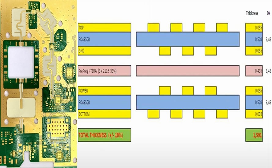
Wire bonding solves the density problem on paper and creates a new one in production. Bonded assemblies are difficult to handle, difficult to test before encapsulation and difficult to reproduce in the quantities a robot programme needs.
Any-Layer HDI Flex as the Enabling Structure
The structure that satisfies the density and the flexibility together is a multi layer any-layer high density interconnect flexible circuit on polyimide, with lines and spaces at fifty micrometres and blind vias of seventy five micrometres.
Any-layer construction allows a via between any pair of adjacent layers, so routing is not forced to escape to the outer layers. That freedom is what makes it possible to distribute hundreds of conductors through a fingertip without widening the part.
Microvia Alignment in Polyimide
Polyimide moves more than rigid laminate during lamination. Its coefficient of thermal expansion runs between twenty and twenty five parts per million per degree, against fourteen to seventeen for ordinary FR-4, and that movement occurs across a stack bonded under heat and pressure.
When expansion is not compensated, layer to layer registration drifts by tens of micrometres. A landing pad for a small blind via cannot absorb that drift, so the result is opens, shorts and a defect rate that climbs into double digits.
Process Changes That Recover Registration
Three measures address the problem together. Laser direct imaging with target and datum compensation tightens exposure alignment; a slower lamination ramp with higher pressure reduces substrate distortion; and a modified low expansion polyimide brings the substrate closer to the copper it carries.
Applied as a set, those changes move registration from roughly thirty five micrometres of drift to about fifteen, and blind via defects fall from more than twenty percent to under two. No single measure is sufficient on its own.
Why Pilot Lots Fall From Prototype Yield
Prototype builds are forgiving because engineers watch every unit and adjust as they go. A pilot lot of a hundred pieces removes that attention, and yield often drops by thirty or forty percentage points at exactly that transition.
The drop is rarely caused by one failure mode. Alignment, bend resilience and impedance spread interact, and improving one while ignoring the others simply moves the loss to a different test step. Manufacturing a flexible sensor circuit at volume therefore calls for PCB manufacturing discipline across the whole sequence.
Bend Life at a 1.5 Millimetre Radius
A finger joint bends through a large angle with a radius of roughly a millimetre and a half, and the product specification may require a hundred thousand cycles. Testing to the standard flex fatigue method, an unoptimised design can fail before ten thousand.
The failure is mechanical rather than electrical. Copper fatigues where tensile strain concentrates, cracks initiate at a surface irregularity, and the conductor eventually opens. Design decisions taken long before the first bend test determine where that happens.
Trace Direction and Copper Selection
Two changes lift bend life substantially. Routing conductors at forty five degrees to the bend line spreads strain across a longer path instead of concentrating it across a perpendicular trace, and choosing rolled annealed copper with high elongation keeps grain structure aligned with the flex direction.
Adding a thin polyimide stiffener layer over the bend region distributes stress as well. Together these measures can take a flexible circuit from a few thousand cycles to well beyond a hundred and fifty thousand.
Coverlay Openings and Stress Concentration
Coverlay defines where the circuit is protected and where it can move, and the boundary between those regions behaves like a notch. If the opening edge falls on the bend line, every cycle loads the same cut edge.
Moving the opening off the bend line by half a millimetre removes that concentration. It is a small layout change with a large effect on fatigue life, and it is far cheaper than changing materials after a field failure. Teams working on flexible board capability treat the bend region as a designed feature rather than an incidental area.
Impedance Consistency Across Batches
Sensing channels routed as controlled impedance lines may target fifty ohms with a plus or minus five ohm window. Holding that window at volume depends on two variables that move independently: dielectric constant and etched line width.
When both drift, the process capability index collapses. A pilot run with an index near 0.9 implies that roughly a third of units fall outside the window, which is exactly the kind of loss that only appears after prototypes have passed.
Incoming Material Control for Dielectric Spread
Polyimide dielectric constant is quoted as a range rather than a number, and incoming material can vary across that range by several tenths. Each value changes the impedance of a fixed geometry.
Binning incoming material by measured dielectric constant and applying a matching etch compensation per bin addresses the cause rather than the symptom. It is a material control measure that outperforms repeated process tuning, because it removes the variation instead of chasing it.
Measuring Impedance on the Line
Verifying impedance only on finished boards leaves too little room to react. Time domain reflectometry monitoring during production feeds line width deviation back to the etch process while the lot is still running.
First article testing across a defined set of coupon positions then confirms that the model still matches reality. That combination supports capability indices above 1.6 and pass rates above ninety nine percent on impedance, which is what a robot programme needs before committing to volume.
Signal Conditioning Beside the Sensor
Raw tactile signals are small and easily disturbed, so amplification and filtering belong close to the sensing element rather than at the end of a long cable. That requirement puts active components inside the fingertip assembly.
Placing devices on a flexible substrate raises assembly difficulty, because the substrate does not hold position during reflow. Carrier fixtures and controlled profiles make the placement repeatable. This is where flexible circuit assembly experience shows in the yield figures.
Noise and Crosstalk in a Crowded Fingertip
Hundreds of conductors running through a confined flexible section sit close to one another. Fast switching on digital lines couples into adjacent analog channels if reference and shielding are not planned layer by layer.
Ground planes between signal groups, careful return path design and separation of analog and digital regions limit that coupling. The constraint is that shielding consumes the same space as routing, so every layer has to earn its place.
Assembling a Flexible Sensor Stack
A finished fingertip is a stack of sensing layer, flexible circuit, stiffener and coverlay, bonded and formed to a curved surface. Bonding pressure, adhesive thickness and alignment between layers all affect both sensitivity and fatigue life.
Because the stack is assembled rather than simply soldered, process control extends beyond the electronics. Suppliers who understand low volume assembly and volume ramp in the same process chain handle this transition more predictably than those who only build bare circuits.
Volume Ramp and Yield Management
Robot programmes move quickly, and a supplier may be asked to support a design freeze, a pilot batch and a production ramp inside a few months. Prototype turnaround measured in days and pilot delivery measured in about a week keep that schedule achievable.
Yield management is what makes the ramp real. Tracking defect modes by process step, holding alignment and impedance capability indices within limits, and reviewing incoming material every lot converts a working design into a shippable product. Programmes that need both speed and control often start with rapid prototyping and then carry the same process parameters into volume.
What the Next Generation Will Ask For
Channel counts will rise, frame rates will increase, and sensing will move from the fingertip pad onto the whole finger surface including the palm. Each step adds conductors to the same limited volume.
The response will be finer features, thinner dielectrics and more layers in the same thickness. Flexible circuit manufacturing is already the narrowest part of the supply chain for dexterous hands, and that position is unlikely to change soon.