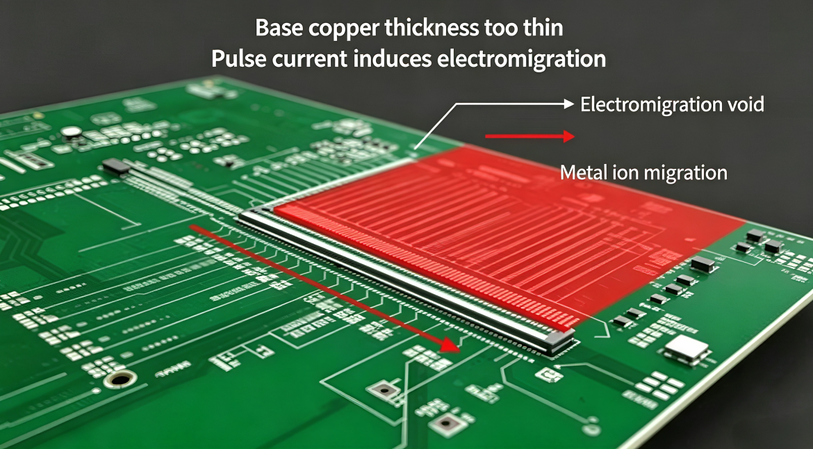
As high-speed memory and processor interfaces continue to increase in bandwidth, PCB designers must pay closer attention to more than routing, impedance, and layer stackup. PCB copper thickness at critical component interfaces can also affect long-term reliability, particularly when BGA packages carry high-density transient or pulse currents.
In applications such as DDR5, GDDR6, FPGA, and high-speed networking hardware, a PCB may experience repeated current pulses through relatively small BGA pad structures. If the copper cross-sectional area is insufficient, local current density can increase significantly. Combined with elevated temperature, humidity, thermal cycling, and intermetallic compound growth, this can contribute to copper consumption and interface degradation.
This article explains how PCB copper thickness, surface finish, BGA pad geometry, current density, and thermal conditions interact, and provides practical guidelines for evaluating electromigration and reliability risks during PCB design and manufacturing.
Why PCB Copper Thickness Matters Under Pulse Current
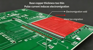
Electromigration refers to the movement of metal atoms driven by the momentum transfer associated with current flow. It becomes increasingly important as current density and operating temperature rise.
For a conventional low-current digital signal, the copper thickness of a PCB trace may not be the dominant reliability factor. However, a BGA power or high-current connection can concentrate current into a small area. The effective cross-sectional area may become even smaller around pad edges, vias, neck-down regions, and surface-finish interfaces.
As a result, two PCB designs with identical nominal electrical specifications can have different reliability margins if their actual copper thickness and current distribution are different.
For high-speed systems, this issue should therefore be considered together with signal integrity, power integrity, thermal management, and mechanical reliability.
How Pulse Current Can Accelerate Copper Consumption
The relationship between current and conductor stress is strongly affected by current density:
J = I / A
where:
- J is current density;
- I is current;
- A is the effective conducting cross-sectional area.
When the available copper area decreases, local current density increases even if the total current remains unchanged.
This is particularly important around BGA pads. Current does not always distribute uniformly across the entire pad. Geometrical transitions can produce current crowding near pad edges, via connections, neck-down areas, or interfaces between different conductive materials.
At elevated temperatures, atomic diffusion also becomes faster. Therefore, repeated pulse-current operation under high-temperature conditions can increase the cumulative stress on copper and intermetallic interfaces.
It is important to distinguish this mechanism from a simple soldering defect. A BGA joint can pass initial electrical testing while still containing a reliability risk that develops during extended temperature, humidity, current, or thermal-cycle exposure.
ENIG Does Not Eliminate Electromigration Risk
ENIG is widely used for BGA pads because its nickel barrier and thin gold layer provide good solderability, surface protection, and storage stability.
However, the presence of a nickel layer does not mean that the underlying copper is immune to current-induced degradation.
The actual reliability margin depends on several factors, including:
- PCB copper thickness
- Nickel thickness
- Pad geometry
- Local current density
- Operating temperature
- Pulse-current amplitude and duration
- Surface-finish process
- Copper grain structure
- Solder alloy and intermetallic growth
- PCB and package CTE mismatch
A thin copper layer provides less material reserve when copper atoms migrate or are consumed during interfacial reactions. If the local current path is also constricted, the effective stress can be considerably higher than that predicted from average board-level current.
Therefore, designers should evaluate the complete conductive structure rather than assuming that ENIG alone provides sufficient protection.
12 μm vs. 20 μm Copper: Why the Difference Matters
Consider a BGA pad where the nominal surface copper thickness is approximately 12 μm compared with another design using approximately 20 μm.
The thicker copper layer provides a larger conductive cross-sectional area and a greater material reserve. Under otherwise comparable conditions, it can reduce the local electrical and thermal stress associated with current crowding.
However, it is not technically correct to state that increasing copper from 12 μm to 20 μm will always produce a specific failure-rate reduction. Actual reliability depends on pad dimensions, current waveform, temperature, stackup, plating process, solder alloy, and package construction.
For this reason, laboratory results showing a large difference between two copper thicknesses should be treated as application-specific validation data, rather than as a universal reliability ratio.
For DDR5 and other high-speed memory interfaces, the more useful engineering question is:
Is the minimum actual copper thickness at the BGA pad sufficient for the application’s peak current, thermal environment, and expected service life?
That question should be answered using electrical analysis, manufacturing capability data, and reliability testing.
Actual Copper Thickness Is More Important Than Nominal Copper Weight
One of the most common PCB manufacturing misunderstandings is confusing copper foil weight with the final copper thickness after processing.
For reference, 1 oz copper is approximately 35 μm before manufacturing processes are considered. However, the final thickness of a PCB conductor can be affected by:
- Copper foil thickness
- Etching
- Plating
- Pattern geometry
- Copper distribution
- Manufacturing tolerances
- Local process variation
Therefore, a designer should not simply specify a copper weight and assume that the same thickness exists everywhere on the finished PCB.
For critical BGA pads, the minimum finished copper thickness may be more meaningful than the nominal starting foil specification.
Surface Finish and BGA Pad Geometry Must Be Evaluated Together
Surface finish can change the conductive structure at the pad interface.
With ENIG, the copper surface is processed before nickel and gold deposition. The preparation process may remove a small amount of copper depending on the manufacturing process.
OSP follows a different process and does not use the same nickel barrier structure. It may therefore behave differently under soldering, thermal cycling, and long-term environmental exposure.
The correct surface finish depends on the application. Designers should consider:
- Required solderability
- Storage requirements
- Pad geometry
- Current load
- Thermal cycling
- Environmental conditions
- Expected product lifetime
- Manufacturer process capability
The surface finish should not be evaluated independently from PCB copper thickness.
BGA Current Crowding Can Increase Local Current Density
Average current density calculations can sometimes hide the most critical area.
For example, if a BGA pad connects to a narrow trace or via structure, the current may be forced through a smaller effective area before spreading into the wider copper plane.
This produces local current crowding.
A simplified engineering workflow should therefore consider:
- Total current through the BGA connection.
- Effective copper cross-sectional area.
- Pad and trace geometry.
- Via arrangement.
- Current spreading into internal planes.
- Temperature distribution.
- Pulse duration and repetition rate.
This is particularly important for high-current power balls located close to high-speed signal balls.
A robust design should minimize abrupt changes in conductor geometry and provide sufficient copper area for current spreading.
High-Speed Interfaces Require Both SI and Reliability Analysis
Modern DDR5, GDDR6, PAM4, and high-speed FPGA designs cannot be evaluated solely by DC resistance.
The same BGA region may simultaneously carry:
- High-speed data signals
- Clock signals
- Power rails
- Ground connections
- High-frequency return currents
- Short-duration transient currents
Consequently, PCB layout must balance signal integrity, power integrity, thermal performance, and manufacturing reliability.
A copper structure that is electrically acceptable under average current may still experience excessive local heating or current crowding during transient operation.
For high-speed systems, designers should review peak and RMS current separately and evaluate whether the copper geometry remains adequate during the worst-case operating condition.
Do Not Confuse Copper Foil Thickness With Finished Copper Thickness
A common design mistake is specifying the starting copper foil without controlling the finished copper at the critical pad.
For example, a design may start with a thicker copper foil and subsequently remove material during etching. Depending on the manufacturing process and feature geometry, the final copper thickness can vary.
For critical BGA structures, the manufacturing drawing should clearly define the required finished copper thickness.
Instead of relying only on statements such as:
“1/2 oz copper”
a more useful requirement may be:
“Finished copper thickness at critical BGA pads: minimum XX μm.”
The exact value should be established according to the current requirement, pad geometry, material system, fabrication capability, and reliability target.
CTE Mismatch Can Magnify BGA Reliability Problems
Electrical stress is only one part of the problem.
A semiconductor package, solder joint, and PCB have different coefficients of thermal expansion. Silicon has a much lower CTE than conventional FR-4 materials, while the PCB and package materials expand and contract differently during temperature changes.
During thermal cycling, this mismatch generates mechanical stress around the BGA solder joints.
If the copper structure is relatively thin or mechanically weak, stress can become concentrated around the copper/nickel/solder interface. Repeated cycling can contribute to:
- Solder-joint fatigue
- Pad cracking
- Interfacial degradation
- Intermetallic growth
- Copper consumption
- Intermittent electrical failures
Therefore, BGA reliability should be evaluated as an interaction between electrical, thermal, and mechanical effects rather than as an isolated copper-thickness problem.
Practical Design Guidelines for DDR5 and High-Speed BGA
For high-speed BGA applications, designers can establish an internal engineering control plan around several parameters.
1. Define Minimum Finished Copper Thickness
For DDR5, GDDR6, FPGA, and other high-density BGA applications, establish a minimum finished copper thickness for critical pads based on the expected current and reliability requirements.
A value such as 18–20 μm may be used as a design target in some applications, but it should not be treated as a universal requirement. The final specification should be validated against the actual current waveform and PCB fabrication process.
2. Check Peak Pulse Current
Do not rely only on average current.
Review the IC or module datasheet for:
- Ipeak
- Pulse duration
- Rise/fall time
- Duty cycle
- Repetition rate
- Maximum operating temperature
Short high-current pulses can create significantly different local stresses from continuous DC current.
3. Verify the Actual BGA Pad Copper
Critical BGA pads should be checked using appropriate manufacturing inspection methods.
Depending on the required accuracy, verification can include:
- XRF measurement
- Microsection analysis
- SEM analysis for failure investigation
- Cross-sectional metallography
- Process capability data
The objective is to confirm the minimum actual copper thickness, rather than simply confirming the nominal material specification.
4. Control Current Crowding
Avoid unnecessary neck-down structures around high-current BGA pads.
Where appropriate, use:
- Multiple vias
- Larger copper areas
- Shorter current paths
- Multiple plane connections
- Symmetrical via structures
- Adequate copper distribution
These measures can help reduce local current density and improve current spreading.
Three Common Engineering Mistakes
Mistake 1: Using Nominal Copper Weight as the Acceptance Criterion
A nominal 1/2 oz or 1 oz specification does not automatically guarantee a specific finished copper thickness at every BGA pad.
The fabrication drawing should define the critical finished-copper requirement.
Mistake 2: Ignoring Pulse Current
A board may operate correctly during normal functional testing while experiencing significantly higher transient current during memory bursts or processor activity.
Peak current should therefore be included in the reliability evaluation.
Mistake 3: Treating Electromigration as a Solder-Only Problem
When a failure occurs near a BGA joint, it is tempting to attribute the problem entirely to soldering.
However, the failure mechanism may involve several interacting factors:
PCB copper → surface finish → solder → IMC → package → thermal cycling
A proper failure analysis should therefore examine the entire interconnection structure.
Recommended Verification Workflow
A practical PCB reliability workflow can be divided into four stages.
Step 1: Electrical Analysis
Determine peak current, RMS current, pulse duration, duty cycle, and effective conductor area.
Step 2: Layout Review
Inspect BGA pad geometry, copper thickness, trace neck-downs, via structures, and power-plane connections.
Step 3: Manufacturing Verification
Confirm finished copper thickness at critical locations using XRF or microsection analysis where appropriate.
Step 4: Reliability Validation
For products with demanding operating environments, conduct appropriate temperature-humidity, thermal cycling, current stressing, or accelerated life testing based on the applicable product qualification requirements.
This approach is more reliable than selecting a copper thickness from a single rule of thumb.
How Kingda Can Support High-Reliability BGA PCB Manufacturing
For high-speed BGA products, PCB copper thickness should be controlled together with pad geometry, stackup, surface finish, via structure, and manufacturing tolerances.
Kingda can incorporate critical copper-thickness requirements into the PCB manufacturing documentation and coordinate them with fabrication and inspection processes.
For designs involving DDR5, GDDR6, FPGA, PAM4, or other high-speed interfaces, engineers should provide key information such as:
- BGA pitch and pad dimensions
- Peak and average current
- Pulse-current characteristics
- Required surface finish
- Minimum finished copper thickness
- PCB material and stackup
- Operating temperature range
- Reliability requirements
This allows the manufacturing process to be evaluated against the actual electrical and mechanical requirements instead of relying only on nominal PCB specifications.
Conclusion
As BGA packages become denser and high-speed interfaces operate at increasingly demanding data rates, PCB copper thickness is becoming an important part of PCB reliability engineering.
Insufficient copper thickness can reduce the available conductive area, increase local current density, and reduce the material margin available under prolonged electrical and thermal stress. When combined with high temperature, surface-finish interfaces, intermetallic growth, and PCB-package CTE mismatch, these factors can contribute to long-term reliability problems.
For DDR5, GDDR6, FPGA, and other high-speed BGA applications, engineers should therefore evaluate electromigration, pulse current, finished copper thickness, current crowding, thermal conditions, and signal integrity as part of a complete design-for-reliability process.
The most practical rule is simple: do not judge critical BGA copper by nominal foil weight alone. Specify, measure, and control the actual finished copper thickness where the current really flows.