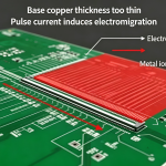
In high-power PCB applications, designers often focus on copper thickness and trace width when evaluating voltage drop. However, these are not the only factors that determine the performance of a power distribution path.
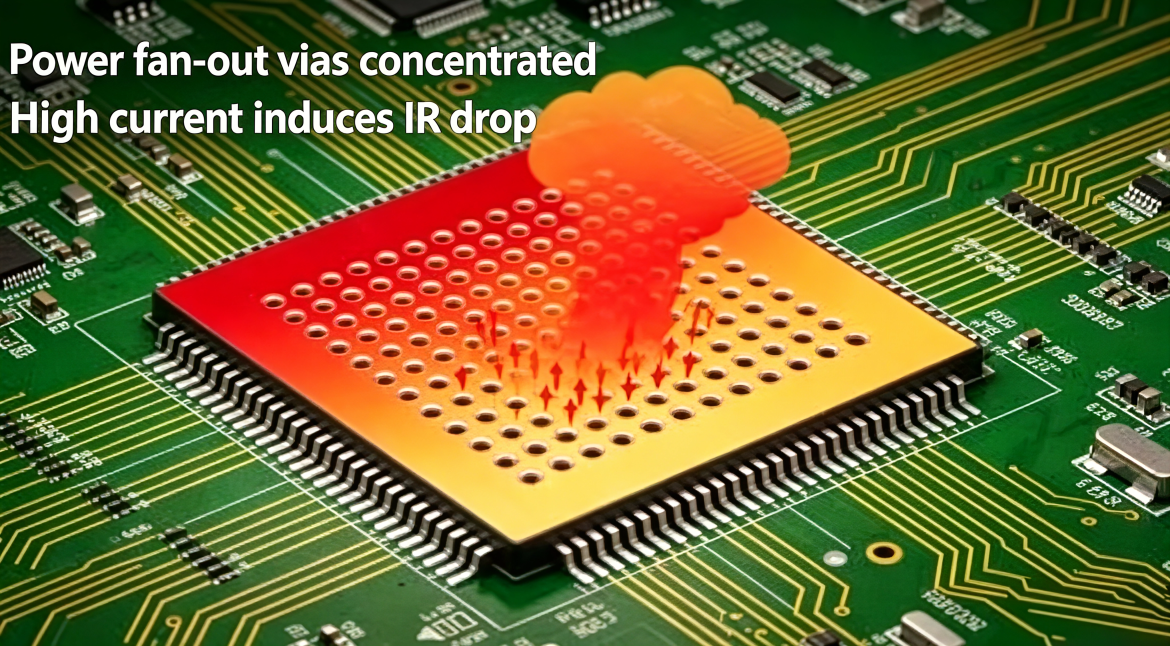
A concentrated group of vias can create a significant bottleneck in a high-current PCB power path. Even when the total number of vias appears sufficient, poor distribution can increase local current density, resistance, and heat generation. The result may be localized IR drop, excessive temperature rise, and long-term reliability problems around power components.
This issue becomes particularly important in DC-DC converters, MOSFET power stages, BGA power packages, servers, industrial power supplies, and other high-current PCB applications.
The key engineering principle is simple:
Via quantity does not directly equal current-carrying capability. Effective conductive area, current distribution, thermal dissipation, and connection quality must all be considered.
Why IR Drop Is Not Uniformly Distributed
IR drop is commonly expressed as:
V = I × R
where:
- V is voltage drop;
- I is current;
- R is the resistance of the current path.
In an idealized PCB, current would distribute evenly through a sufficiently large copper area. In an actual design, however, current distribution is affected by trace geometry, via layout, pad dimensions, copper thickness, plane transitions, and connection resistance.
When many vias are packed into a small region, current may be forced through a relatively restricted conductive area.
This creates localized current density.
Higher current density increases resistive power dissipation:
P = I²R
The resulting heat can further increase conductor resistance and create a localized thermal feedback effect.
Therefore, a power fanout region should not be evaluated only by counting the number of vias. The entire three-dimensional current path must be considered.
Via Quantity Does Not Equal Via Current Capacity
A common PCB design assumption is that adding more vias will automatically solve a high-current problem.
In practice, via current capacity depends on multiple parameters:
- Finished hole diameter
- Copper plating thickness
- Via barrel length
- Copper distribution
- Connection to internal planes
- Pad geometry
- Via spacing
- Operating temperature
- Thermal coupling between adjacent vias
- Manufacturing tolerances
For example, a group of small vias concentrated within a very small area may provide less practical via current capacity than the same number of vias distributed across a larger copper region.
This is because the electrical resistance of the complete path includes more than the via barrels themselves.
The connection from the component pad to the via, the via-to-plane transition, and the copper spreading resistance all contribute to the total impedance.
How Concentrated Vias Increase Current Density
Consider a high-current BGA or power-component fanout where multiple vias are placed within a compact region.
If the total current remains constant while the effective conductive cross-sectional area becomes smaller, local current density increases.
A simplified relationship is:
J = I / A
where J represents current density and A represents the effective conductive area.
For this reason, simply increasing the number of vias without increasing the effective current-spreading area may provide diminishing returns.
A better strategy is to distribute the current through multiple parallel paths and connect those paths efficiently to the internal power planes.
Where PCB space permits, designers should avoid creating a single dense via cluster directly beneath a high-current pad unless electrical and thermal analysis confirms that the structure is adequate.
Via Spacing and Thermal Coupling
Via spacing affects both electrical current distribution and thermal performance.
When high-current vias are placed extremely close together, their thermal fields overlap. The resulting temperature rise may be higher than that predicted by evaluating each via independently.
The exact derating factor depends on:
- Via diameter
- Plating thickness
- Board thickness
- Copper plane configuration
- Ambient temperature
- Via-to-via spacing
- Total current
- Duty cycle
Therefore, fixed spacing rules should be treated as design guidelines rather than universal acceptance criteria.
For a high-current PCB application, the more useful question is whether the complete via group can carry the required current while maintaining an acceptable temperature rise under worst-case operating conditions.
Distributed Via Layout Can Improve Current Spreading
One practical approach is to distribute vias rather than concentrating them into one compact cluster.
For example, instead of placing twelve small vias in a single dense region, the designer may divide them into several groups and connect each group to a broader copper area.
This can provide several benefits:
- More uniform current distribution
- Lower local resistance
- Reduced current crowding
- Better heat spreading
- Lower localized temperature rise
- Improved manufacturing robustness
The optimum via layout depends on the available routing area and the electrical structure of the PCB.
The goal should not be to maximize the physical distance between every via. Instead, the goal is to create multiple low-resistance current paths without introducing unnecessary inductive or resistive bottlenecks.
Copper Thickness Alone Cannot Solve a Poor Via Layout
Increasing copper thickness can reduce resistance, but it cannot completely compensate for a poorly designed via layout.
For example, a 2 oz copper plane may provide a very low-resistance path across a large area. If the current enters that plane through a small group of undersized or poorly distributed vias, however, the via transition can become the dominant resistance.
This is why high-current PCB analysis should evaluate the complete path:
Component pad → fanout → vias → internal power plane → vias → load
The highest-resistance section of this path often determines the actual IR drop.
A wide trace connected to a poorly distributed via field may therefore perform worse than expected.
Power Distribution Should Be Designed as a Three-Dimensional Network
Modern power PCBs are no longer simple two-dimensional structures.
Current frequently moves:
- From a surface pad into a via field
- Through multiple PCB layers
- Across internal copper planes
- Through another via field
- Into the load or return path
This makes power distribution a three-dimensional network.
During PCB design, engineers should therefore inspect transitions between layers rather than analyzing only individual traces or planes.
For high-current DC-DC converters, special attention should be given to:
- MOSFET drain/source connections
- Inductor current paths
- Input and output capacitor connections
- Ground return structures
- BGA power balls
- Thermal vias
- Power-plane transitions
A short and wide copper path is useful, but only when the vertical transitions can support the same current level.
Thermal Management Is Part of Current-Carrying Design
Electrical and thermal performance are closely linked.
As current flows through a resistive path, heat is generated according to:
P = I²R
If the generated heat cannot be removed efficiently, local temperature rises. Higher temperature can increase copper resistance and accelerate thermal stress on solder joints, vias, pads, and laminates.
Therefore, PCB thermal management should be considered at the same time as electrical current capacity.
Effective PCB thermal management strategies may include:
- Larger copper planes
- Multiple thermal vias
- Distributed power vias
- Larger copper areas around power components
- Improved connection to internal copper planes
- Adequate board-level heat spreading
- Appropriate component placement
For high-power applications, thermal simulation or infrared measurements can help identify hotspots that may not be obvious from DC voltage-drop calculations alone.
Do Not Rely Only on DC IR-Drop Simulation
A DC IR drop simulation is useful, but it does not necessarily reveal every long-term reliability issue.
A design may show an acceptable initial voltage drop while still experiencing localized heating or mechanical stress after repeated power cycling.
The analysis should therefore consider:
- DC resistance.
- Peak current.
- RMS current.
- Pulse duration and duty cycle.
- Temperature distribution.
- Thermal cycling.
- Mechanical stress.
- Via and pad manufacturing quality.
For high-current switching power supplies, transient behavior should also be evaluated because instantaneous current distribution can differ from the steady-state condition.
Manufacturing Quality Can Affect Via Current Capacity
The electrical performance of a via depends not only on its nominal dimensions but also on its actual manufacturing quality.
Important parameters include:
- Finished hole diameter
- Plated copper thickness
- Barrel continuity
- Pad connection
- Void formation
- Registration accuracy
- Drill quality
- Copper-to-pad interface
A localized defect in the via barrel or connection can increase resistance and create an unexpected hotspot.
For high-current applications, PCB manufacturers should therefore establish appropriate process controls and inspection methods for critical via structures.
Depending on product requirements, inspection may include:
- Microsection analysis
- X-ray inspection
- Electrical continuity testing
- Plating-thickness verification
- Cross-sectional metallography
The inspection method should match the failure mechanism being investigated.
Material and Stackup Also Influence Thermal Performance
Standard FR-4 materials are widely used in power PCBs, but their thermal conductivity is relatively limited compared with dedicated thermal-management materials.
The actual thermal performance depends on:
- Laminate construction
- Resin content
- Copper coverage
- Board thickness
- Internal copper planes
- Thermal vias
- Component power dissipation
- Airflow
For high-power designs, simply changing to a high-frequency or specialty laminate should not be assumed to solve a thermal problem.
Material selection should be based on the complete electrical, thermal, mechanical, and manufacturing requirements.
Common High-Current Via Design Mistakes
Mistake 1: Counting Vias Instead of Calculating the Current Path
Twelve vias do not necessarily provide twelve times the performance of one via.
The complete conductive path must be evaluated, including pad-to-via transitions and connections to internal copper planes.
Mistake 2: Placing Too Many Vias in One Small Area
A dense via cluster can create current crowding and thermal coupling.
If sufficient board space is available, distributing the vias can improve current spreading and thermal uniformity.
Mistake 3: Increasing Copper Thickness Without Reviewing the Via Field
A thicker copper plane can reduce planar resistance, but the benefit may be limited if the current still enters through a restricted via structure.
Mistake 4: Checking Only Initial Voltage Drop
Initial electrical testing does not necessarily reveal degradation caused by thermal cycling or repeated power switching.
Long-term reliability should be evaluated when the product operates under demanding thermal and electrical conditions.
Practical Design Guidelines for High-Current PCB Fanout
For high-current power fanout structures, the following workflow is recommended.
1. Calculate the Required Current Path
Determine:
- Maximum continuous current
- Peak current
- RMS current
- Pulse duration
- Duty cycle
- Maximum operating temperature
Do not size the via structure from average current alone.
2. Calculate Effective Conductive Area
Evaluate the combined conductive area of:
- Via barrels
- Pads
- Traces
- Copper planes
- Layer transitions
The smallest effective section of the current path may become the critical bottleneck.
3. Review Via Layout
Check whether the vias are concentrated excessively around a single point.
Where practical, distribute the vias across a larger copper region and provide multiple connections to the internal power plane.
4. Verify Thermal Performance
Use thermal simulation, temperature measurements, or both to identify localized hotspots.
The design target should be based on the actual component temperature limit and system reliability requirements.
5. Verify Manufacturing Capability
Confirm that the selected via diameter, aspect ratio, plating thickness, pad geometry, and copper thickness are compatible with the PCB manufacturer’s process capability.
This step is especially important when using large copper areas, high-current vias, or tightly packed BGA fanout structures.
What to Do When Board Space Is Limited
Sometimes the power component or BGA package leaves insufficient space for a widely distributed via pattern.
In this situation, several options can be evaluated:
- Increase via diameter
- Increase via plating thickness
- Add additional copper layers
- Use multiple power planes
- Increase copper area around the fanout
- Optimize pad-to-via geometry
- Relocate noncritical signals
- Use alternative via structures where appropriate
A larger via is not automatically the best solution. Its drill size, aspect ratio, pad size, manufacturing cost, and interaction with the component footprint must all be considered.
The correct solution is the one that improves the complete electrical and thermal path while remaining manufacturable.

Kingda’s Approach to High-Current PCB Via Design
For high-current PCB projects, Kingda recommends evaluating via layout, copper thickness, power-plane structure, thermal performance, and manufacturing tolerances together.
During engineering review, key information should include:
- Maximum continuous current
- Peak pulse current
- Component package type
- BGA pitch where applicable
- PCB layer count
- Copper thickness
- Via diameter
- Via plating requirements
- Surface finish
- Operating temperature
- Thermal requirements
- Reliability targets
Kingda can use these requirements to assess the manufacturability of high-current via structures and help ensure that the final PCB design provides a practical balance between electrical performance, PCB thermal management, reliability, and production capability.
Conclusion
High-current PCB performance is determined by more than trace width and copper thickness.
When power vias are concentrated into a small fanout region, local current density can increase and create additional resistance and heat generation. The resulting IR drop may become significantly higher in the fanout area than the average voltage drop across the PCB.
For this reason, designers should treat via current capacity, via layout, and power distribution as part of one integrated design problem.
The most effective approach is not simply to add more vias. Instead, engineers should create multiple low-resistance current paths, distribute current effectively, provide sufficient copper for heat spreading, and verify the finished structure through both electrical and thermal analysis.
For demanding DC-DC, BGA, server, industrial, and high-power applications, early coordination between PCB design and manufacturing is essential. A well-designed via layout can reduce localized voltage drop, control temperature rise, and improve the long-term reliability of the complete power delivery network.