Portable life-monitoring equipment such as ECG, SpO₂, temperature, and respiration monitors places demanding requirements on PCB design. Physiological signals can be only millivolt- or microvolt-level at the sensing interface, making them highly susceptible to interference from digital switching, power conversion, wireless communication, and external electromagnetic fields.
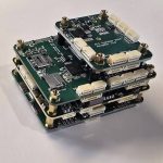
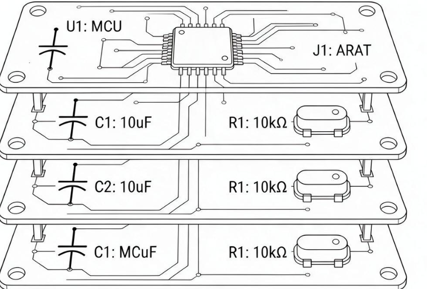
For these applications, a carefully designed 4-layer PCB can provide a practical balance between electrical performance, board size, manufacturing complexity, and cost. Compared with a two-layer design, a four-layer structure provides more opportunities to establish continuous reference planes, control return-current paths, separate power distribution from signal routing, and improve signal integrity. At the same time, it can be less complex than a six-layer structure for compact, cost-sensitive medical monitoring products.
However, simply increasing the number of PCB layers does not automatically solve noise problems. The PCB stackup, material construction, reference-plane arrangement, component placement, and routing strategy must work together.
Project Background and Key Design Constraints
The customer developed a battery-powered home ECG monitoring device. The product needed to acquire ECG signals from the human body while integrating an MCU, Bluetooth communication, and lithium-battery power management on the same board.
The original design used a two-layer PCB. During prototype debugging, significant noise appeared in the ECG waveform. Baseline drift was also observed, and the acquisition performance did not meet the project’s target requirements.
The engineering team therefore evaluated a four-layer architecture.
The primary objectives were to create sufficient physical separation between the analog front end, digital processing, power circuitry, and reference plane while keeping the PCB within approximately 60 mm × 40 mm to satisfy the mechanical constraints of the portable enclosure.
The major design constraints included:
- 3.7 V lithium-battery power
- Low-power operation
- High input impedance at the analog front end
- Very low-level physiological signal acquisition
- Bluetooth wireless communication
- MCU and digital processing circuitry
- Battery charging and protection circuitry
- Medical-device insulation and solderability requirements
- Consistent electrical performance between production boards
The central engineering question was not simply how to add more copper or more filtering. It was how to construct a PCB stackup that gives sensitive analog signals a stable reference while preventing noisy digital and power currents from unnecessarily interacting with the acquisition circuitry.
Comparing Two Common 4-Layer PCB Stackups
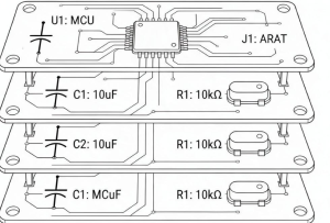
Two four-layer configurations were considered during the design evaluation.
Stackup A: Signal / Ground / Power / Signal
The first configuration was:
Layer 1: Signal
Layer 2: GND
Layer 3: Power
Layer 4: Signal
The top layer was primarily used for connectors and analog acquisition circuitry. A relatively continuous ground plane was placed directly underneath the top signal layer.
The power plane occupied the third layer, while digital circuitry and selected communication routing could be placed on the bottom layer.
One major advantage of this structure is that sensitive top-layer analog traces can reference the adjacent ground plane. When the trace geometry and reference plane are properly designed, the return current has a relatively direct path beneath the signal.
This can reduce unnecessary current-loop area and help limit electromagnetic coupling.
The close proximity between the power and ground layers can also provide useful distributed capacitance. However, the effectiveness of this structure depends on dielectric thickness, plane geometry, material properties, and the frequency range of interest. It should not be treated as a substitute for local decoupling or dedicated power-integrity design.
Stackup B: Signal / Power / Ground / Signal
The second configuration was:
Layer 1: Signal
Layer 2: Power
Layer 3: GND
Layer 4: Signal
This arrangement can be suitable for many digital designs, but it requires careful evaluation when sensitive analog signals are routed on the top layer.
If a critical analog trace primarily references a power plane rather than a continuous ground reference, its return-current behavior may become less predictable. Noise on the power plane can also become part of the electromagnetic environment seen by the signal.
However, this does not mean that the second configuration is inherently unsuitable for every mixed-signal PCB. With appropriate routing, reference-plane planning, impedance control, and power filtering, other four-layer structures can also perform well.
For this project, the engineering evaluation favored Stackup A because it provided a more direct ground reference for the sensitive analog acquisition traces and simplified the intended return-current paths.
Why the Ground Reference Matters
The most important benefit of the selected structure was the continuous reference for sensitive signals.
A signal trace does not exist electromagnetically by itself. Its return current flows through the associated reference structure, and the geometry of this signal-return pair influences loop inductance, electromagnetic coupling, and signal integrity.
For sensitive ECG acquisition circuits, the input signals are particularly vulnerable because they are amplified before they reach a high signal level.
A poorly planned return path can allow digital switching currents to flow through areas associated with the analog front end. This can introduce common-impedance coupling and increase the possibility of interference.
By placing a continuous ground plane close to the primary analog routing layer, the design provides a more predictable reference and return-current environment.
Dielectric Thickness and Stackup Optimization
Once the layer arrangement was selected, dielectric thickness became another important design parameter.
The distance between a signal trace and its reference plane affects several electrical characteristics, including:
- Characteristic impedance
- Electric-field distribution
- Trace-to-plane capacitance
- Return-current distribution
- Electromagnetic coupling
- Effective loop area
A smaller signal-to-reference-plane spacing generally strengthens electromagnetic coupling between the trace and reference plane, which can help confine the field and reduce loop area.
However, thinner dielectric structures can introduce manufacturing and mechanical considerations. Layer registration, lamination control, material tolerance, and the required finished impedance must all be evaluated.
In the project example, a conventional FR-4 construction was considered, with approximately 0.12 mm dielectric spacing between the top signal layer and the internal ground reference and approximately 0.2 mm between the power layer and bottom signal layer.
These values should be regarded as project-specific stackup examples rather than universal design rules. The final dielectric thickness should be calculated together with copper thickness, trace width, target impedance, laminate characteristics, fabrication tolerances, and the PCB manufacturer’s actual process capability.
Do Not Automatically Split the Ground Plane
Another important design decision involved the ground plane.
Engineers sometimes attempt to isolate analog and digital circuits by physically cutting the ground plane into separate analog and digital sections and connecting them at a single point.
This approach can work in specific system architectures, but it is not automatically beneficial for a compact mixed-signal board.
A ground-plane split can create a discontinuity beneath a signal trace. If a high-frequency signal crosses the split, its return current may be forced to travel around the discontinuity instead of following a short path beneath the trace.
The resulting increase in loop area can create additional electromagnetic coupling.
For this 4-layer PCB, the design therefore used a continuous ground reference while implementing functional separation through component placement and routing.
The analog acquisition circuitry was concentrated on one side of the PCB, while the MCU, Bluetooth circuitry, and other relatively noisy digital circuits were placed on the opposite side.
An intentional separation region was maintained between these functional blocks.
This approach provides physical zoning without unnecessarily disrupting the reference plane.
Physical Placement of the Analog Front End
The analog signal integrity of a medical monitoring device is strongly influenced by component placement.
The first amplification stage should be located as close as practical to the sensor interface. The purpose is to minimize the length of the high-impedance, low-level signal path before amplification.
The layout should consider:
- Electrode or sensor connector placement
- Instrumentation amplifier location
- Input protection
- RC filtering
- Reference circuitry
- ADC placement
- Analog power distribution
- Digital-clock proximity
- Wireless-module proximity
High-impedance inputs should not be routed through areas containing high-speed digital signals or RF circuitry.
The shorter and more controlled the sensitive input path is, the fewer opportunities there are for unwanted coupling.
Separating Digital Noise from Analog Acquisition
Digital circuits generate rapidly changing currents whenever internal logic switches.
MCUs, memory devices, clocks, interfaces, and wireless communication circuits can therefore become significant noise sources.
The problem is not simply that digital circuits “make noise.” The more important issue is where their current returns through the PCB.
A well-designed layout should prevent large or rapidly changing digital return currents from unnecessarily flowing through the analog acquisition area.
For this reason, the digital section was placed away from the ECG input and analog front end.
Clock traces were also kept short and controlled where practical. High-speed digital routing was kept away from sensitive analog inputs, while the continuous reference plane provided a predictable return environment.
Power Distribution and Battery Transient Control
The power architecture is another major contributor to analog noise.
The product used a lithium battery, meaning the supply network had to accommodate both relatively stable analog loads and rapidly changing digital or wireless loads.
When a Bluetooth module transmits, its current consumption can change quickly. If the power-distribution network has excessive impedance, these current variations can create voltage fluctuations.
Those fluctuations can then couple into sensitive analog circuits through shared supply paths.
The design therefore separated the power branches according to functional requirements.
The analog front end received a dedicated regulated supply path where appropriate, while digital and RF circuits used their own power branches.
Local decoupling capacitors were placed close to IC power pins to reduce high-frequency supply impedance.
The exact capacitor value and package should be selected according to the device manufacturer’s recommendations and the actual power-distribution network rather than applying one capacitor value universally.
Bluetooth and Wireless Circuit Placement
Wireless communication creates a special challenge for compact medical monitoring boards.
The Bluetooth module and antenna should be located as far as practical from sensitive analog inputs.
The antenna area should follow the module or antenna manufacturer’s recommended keep-out and reference-plane requirements.
Important considerations include:
- Keep the antenna away from ECG inputs.
- Avoid routing sensitive analog traces through the RF area.
- Follow the specified antenna keep-out geometry.
- Minimize unnecessary metal near the antenna.
- Keep RF transmission paths short.
- Maintain the intended reference structure for RF traces.
- Consider the influence of the enclosure and battery.
Wireless interference should be evaluated in the complete mechanical assembly because the enclosure, battery, display, cables, and connectors can all affect RF behavior.
Stackup and Signal Integrity Are Closely Related
The selected stackup also affects impedance and high-speed signal behavior.
For controlled-impedance traces, the relationship between trace width, copper thickness, dielectric thickness, and dielectric constant determines the approximate characteristic impedance.
Therefore, stackup selection should be completed before finalizing critical routing dimensions.
For example, if the reference plane is moved farther away from a signal layer, the same trace width may produce a different impedance. Changing laminate material or dielectric thickness can also change the electrical field distribution.
This is why the PCB stackup should not be treated as a mechanical layer arrangement only.
For medical monitoring products containing Bluetooth, USB, SPI, high-speed clocks, or other fast interfaces, the stackup should be evaluated for both sensitive analog signals and high-speed digital requirements.
Prototype Verification and Engineering Results
After the redesign from a two-layer structure to the selected four-layer architecture, the revised prototype showed a significant reduction in ECG baseline disturbance during evaluation.
The measured power-related and common-mode noise behavior also improved toward the project’s design targets.
Compared with the original two-layer prototype, the project reported an improvement of more than 20 dB in measured signal-to-noise performance under its specified test conditions.
The four-layer construction also provided additional routing space and a more structured power-distribution architecture. Battery-load transients produced less noticeable disturbance in the analog supply under the evaluated conditions.
These numerical results are specific to the project, test setup, operating conditions, measurement bandwidth, and instrumentation. They should not be interpreted as universal performance improvements for every four-layer medical PCB.
The broader engineering lesson is that the layer count itself is not the primary solution. The improvement resulted from the combination of stackup selection, ground referencing, physical zoning, power distribution, and routing discipline.
Practical 4-Layer PCB Stackup Design Workflow
For similar medical monitoring projects, the following workflow can improve design consistency.
1. Identify Sensitive and Noisy Circuits
Classify the major circuit blocks before placement:
- Low-level analog acquisition
- Precision references
- ADCs
- MCU and digital logic
- Wireless communication
- Power conversion
- Battery management
- External interfaces
2. Establish the Layer Architecture
Determine which layers will carry signals, power, and ground.
Give priority to providing sensitive signal layers with an appropriate continuous reference.
3. Define the Material Stackup
Specify:
- Laminate type
- Dielectric thickness
- Copper thickness
- Finished board thickness
- Target impedance
- Manufacturing tolerances
The fabricator should verify whether the proposed stackup is compatible with actual production capability.
4. Place the Analog Front End First
Locate sensor connectors, protection components, amplifiers, filters, references, and ADC-related circuitry before placing noisy digital components.
5. Create Physical Functional Zones
Separate analog, digital, RF, and power functions spatially while maintaining appropriate reference-plane continuity.
6. Review Return-Current Paths
For every critical signal, ask where its return current flows.
This is particularly important for:
- ECG inputs
- ADC signals
- Clock traces
- RF transmission lines
- High-speed digital interfaces
7. Optimize Power Distribution
Separate sensitive analog supplies from noisy switching and RF loads where appropriate.
Use local decoupling and filtering based on actual circuit behavior.
8. Verify Under Real Operating Conditions
Testing should include relevant worst-case operating states, such as wireless transmission, high MCU activity, battery charging, and simultaneous operation of major subsystems.
A PCB that performs well when Bluetooth is disabled may behave differently when the RF transmitter is active.
Kingda’s Support for Medical PCB Projects
For high-reliability medical electronics, the PCB manufacturer should be involved in the engineering process early enough to evaluate manufacturability and electrical requirements together.
Kingda can support the development and manufacturing of medical and high-reliability PCBs, including projects involving multilayer construction, fine traces, controlled impedance, sensitive analog circuits, wireless communication, and demanding reliability requirements.
During the engineering stage, key areas can include:
- 4-layer PCB stackup evaluation
- Material and dielectric selection
- Controlled-impedance design
- Layer-registration considerations
- Fine-line manufacturing
- Via and hole-size verification
- Copper distribution
- Solder mask requirements
- Prototype-to-production consistency
- Manufacturing process capability
A practical stackup should balance electrical performance with manufacturing capability. An electrically attractive design that is difficult to manufacture consistently may create more risk than a slightly less aggressive structure with a larger process margin.
Conclusion
For portable life-monitoring equipment, the PCB stackup is an important part of the overall noise-control strategy.
The case demonstrates that a well-planned 4-layer PCB can provide a useful balance between cost, board size, routing density, power distribution, and signal integrity.
For sensitive physiological signal acquisition, the key is not simply separating analog and digital circuits by drawing boundaries on the PCB. Engineers must also provide appropriate reference planes, control return-current paths, minimize high-impedance routing, manage power distribution, and keep strong RF or digital noise sources away from sensitive inputs.
A continuous ground plane, when appropriate for the system architecture, can provide a predictable reference without introducing unnecessary return-path discontinuities. Functional zoning can then provide additional isolation while preserving the integrity of the reference structure.
For cost-sensitive medical monitoring products, carefully optimizing the four-layer architecture can provide a practical path toward stable low-level signal acquisition without automatically moving to a more complex multilayer design.
Kingda can work with engineering teams from stackup evaluation and prototype development through PCB manufacturing, helping translate electrical requirements into a practical and production-ready board structure.