In addition to optimizing the PCB design itself, manufacturers can often improve production efficiency by reviewing the PCB manufacturing process for unnecessary or duplicated via-related operations. In mass production, applying the same intensive process and inspection requirements to every via may increase manufacturing time, material consumption, and production costs without providing proportional reliability benefits.
A more practical approach is to establish a risk-based via quality control strategy. By differentiating critical vias from standard vias, optimizing process parameters, eliminating genuinely redundant operations, and maintaining appropriate inspection coverage, manufacturers can improve production efficiency while maintaining the reliability required by the application.
However, process simplification should never mean simply removing quality controls. The appropriate process must be determined by via structure, electrical requirements, aspect ratio, copper thickness, board material, reliability requirements, and applicable specifications.
1. Identifying Redundant Processes in Mass-Production Via Manufacturing
In conventional PCB mass production, manufacturers may apply similar process requirements to vias with very different functional and reliability requirements. Critical power vias, BGA vias, high-speed signal vias, and ordinary signal vias may therefore receive unnecessarily similar levels of processing and inspection.
This one-size-fits-all approach can create several problems.
First, excessive processing increases chemical consumption, equipment utilization, labor requirements, and production time. Second, unnecessary mechanical or chemical treatment can introduce additional process variation. Third, performing identical inspection procedures on every feature may reduce production efficiency when the inspection method does not provide meaningful additional quality information.
For example, a via carrying a critical power current or located in a high-reliability BGA structure may require tighter process control than a standard signal via with relatively low electrical and mechanical stress.
The objective of via process optimization is therefore not to reduce quality standards arbitrarily. Instead, it is to allocate manufacturing and inspection resources according to actual risk.

2. Establishing a Risk-Based Via Process Classification
A practical approach is to divide vias into different process-control categories according to their electrical, thermal, mechanical, and reliability requirements.
Critical Vias
Critical vias may include:
- High-current power vias
- High-voltage vias
- BGA vias with demanding reliability requirements
- High-speed or RF signal vias
- Vias with high aspect ratios
- Vias exposed to significant thermal cycling
- Vias used in automotive, aerospace, industrial, or other high-reliability applications
These structures should receive tighter process control. Depending on the design and applicable standards, manufacturers may need controlled drilling, desmear, electroless copper deposition, controlled via plating, cross-section verification, electrical testing, and enhanced process monitoring.
For high-reliability products, inspection requirements should be determined through engineering risk assessment rather than simply being removed to reduce cost.
Standard Vias
Standard signal and ground vias in conventional applications may have less demanding reliability requirements. When their design dimensions and manufacturing specifications fall within established process capabilities, manufacturers can use mature, standardized process parameters instead of applying unnecessary additional operations.
This may include optimized drilling parameters, standardized desmear conditions, controlled copper plating, and appropriate electrical testing.
The key principle is:
Critical vias receive enhanced control, while standard vias use stable and qualified processes.
This approach can improve manufacturing efficiency without compromising essential reliability requirements.
3. Optimize Drilling and Hole-Wall Preparation
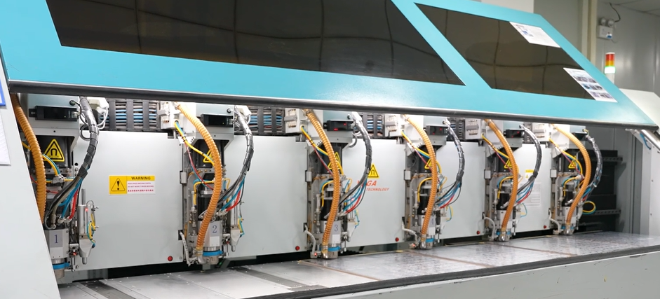
Drilling is one of the fundamental operations in PCB via manufacturing, and stable drilling parameters are essential for consistent hole-wall quality.
Manufacturers should establish qualified drilling parameters based on:
- PCB material
- Board thickness
- Hole diameter
- Aspect ratio
- Copper thickness
- Drill bit type
- Spindle speed
- Feed rate
- Tool life
- Hole-wall quality requirements
Overly aggressive drilling conditions may increase burrs, smear, hole-wall roughness, or thermal damage. Conversely, excessively conservative parameters may reduce productivity and increase tool consumption.
The goal is to identify a stable process window rather than simply selecting the most aggressive or most conservative setting.
Desmear is equally important. Resin smear generated during drilling must be appropriately removed so that reliable copper-to-copper interconnection can be established during subsequent metallization.
However, excessive chemical treatment is not automatically beneficial. Over-processing can alter the resin surface or affect dimensional stability. Therefore, desmear conditions should be validated according to the laminate system and production process.
4. Optimize Via Plating Instead of Simply Increasing Copper Thickness
Copper plating is one of the most important steps affecting through-hole reliability.
The copper deposited on the hole wall must provide a reliable electrical and mechanical connection throughout the service life of the PCB. Plating quality depends on factors such as current density, plating time, bath chemistry, agitation, temperature, panel loading, hole geometry, and aspect ratio.
Simply increasing plating time or copper thickness is not an efficient substitute for process control. Excessive plating may increase material consumption, cycle time, and dimensional variation without providing a proportional reliability improvement.
Instead, manufacturers should establish qualified plating windows that meet the required copper thickness and distribution specifications.
For standard production, a stable process with proven parameters can reduce unnecessary adjustments and improve repeatability. Critical structures may require additional monitoring or verification depending on the product’s reliability class.
5. Simplify Inspection Without Eliminating Essential Quality Controls
Inspection is another area where manufacturers can improve efficiency through risk-based management.
Not every inspection method provides the same value for every PCB structure. Depending on the product, manufacturers may use automated electrical testing, AOI, dimensional inspection, microsection analysis, process monitoring, or sampling inspection.
For standard vias produced within a qualified process window, automated electrical testing and process monitoring may provide sufficient routine control. More detailed destructive analysis, such as microsection inspection, can be performed at an appropriate sampling frequency or when required by the product specification.
For critical vias or products with demanding reliability requirements, additional verification may be necessary.
Therefore, the correct principle is not:
“Remove inspection from standard vias.”
It is:
“Use the appropriate inspection method and frequency for the actual risk level.”
This distinction is important because reducing redundant inspection is different from reducing necessary quality assurance.
6. Standardize Process Parameters to Reduce Manufacturing Variation
Effective PCB cost reduction requires stable processes rather than simply removing production steps.
Manufacturers should establish documented process windows for key operations, including:
- Drill speed and feed rate
- Drill bit replacement criteria
- Desmear parameters
- Electroless copper conditions
- Electroplating current density
- Plating time
- Bath temperature and chemistry
- Copper thickness requirements
- Inspection frequency
- Sampling plans
- Process acceptance criteria
Once qualified parameters have been established, unnecessary manual adjustments should be minimized.
Statistical process control (SPC) can also be used to monitor important manufacturing characteristics and identify process drift before it develops into a larger quality problem.
This approach helps convert individual operator experience into repeatable manufacturing capability.
7. Use Sampling and Process Monitoring for Stable Mass Production
For high-volume production, 100% destructive inspection is obviously impractical. A combination of automated testing, process monitoring, and statistical sampling can provide a more efficient quality-control structure.
For example, manufacturers can monitor key characteristics such as:
- Hole diameter
- Hole-wall copper thickness
- Electrical continuity
- Insulation resistance where applicable
- Registration accuracy
- Hole-wall appearance
- Plating distribution
- Drill quality
Microsection analysis can be used periodically or according to the control plan to verify internal structure and plating quality.
When process capability is demonstrated and remains stable, inspection frequency can be optimized according to the product’s quality plan and applicable standards.
If abnormal trends appear, the inspection level can be increased and the relevant process parameters investigated.
8. Reliability Must Remain the Boundary of Process Simplification
Process simplification should never compromise the fundamental reliability requirements of a PCB.
For products exposed to high temperature, humidity, thermal cycling, high voltage, vibration, or repeated mechanical stress, via reliability may become a critical failure factor.
Engineers should therefore evaluate the relationship between via structure and application conditions before reducing any process or inspection requirement.
Particular attention should be given to:
- High aspect-ratio holes
- Large thermal cycling ranges
- High-current applications
- High-voltage insulation requirements
- Lead-free assembly temperatures
- Automotive and industrial environments
- Flexible or rigid-flex structures
- High-reliability multilayer boards
For these applications, process simplification should be based on qualification data, process capability, reliability testing, and applicable IPC or customer requirements.
9. Quantifying the Benefits of Via Process Optimization
A well-designed via process optimization program can reduce manufacturing costs by improving process stability and removing unnecessary operations.
Potential benefits include:
- Shorter production cycle time
- Lower chemical consumption
- Reduced copper and consumable usage
- Lower equipment utilization
- Reduced manual inspection workload
- Fewer unnecessary process adjustments
- Improved process consistency
- Better production capacity utilization
However, actual savings depend on PCB layer count, via density, board size, production volume, material system, equipment configuration, inspection requirements, and factory process capability.
Therefore, cost-saving percentages should be determined from actual production data rather than treated as universal values.
10. A Practical Framework for Efficient PCB Via Manufacturing
For manufacturers seeking to simplify the PCB manufacturing process, a practical workflow can be summarized as follows:
Step 1: Classify the vias
Identify critical, standard, and application-specific vias according to electrical and reliability requirements.
Step 2: Review every process step
Determine whether each drilling, desmear, plating, inspection, and finishing operation provides a measurable quality benefit.
Step 3: Establish qualified process windows
Define stable parameters for drilling, desmear, metallization, and via plating.
Step 4: Apply risk-based inspection
Use automated inspection, electrical testing, sampling, and destructive analysis according to the actual risk level.
Step 5: Monitor process capability
Use SPC and production data to identify process drift and prevent recurring defects.
Step 6: Verify reliability
For demanding applications, confirm that process changes continue to meet electrical, mechanical, thermal, and environmental reliability requirements.
Step 7: Continuously improve
Use production data to identify additional opportunities for cycle-time reduction, material savings, and quality improvement.
Conclusion
Efficient PCB via manufacturing is not achieved by simply removing process steps. The more effective strategy is to eliminate genuinely redundant operations while retaining the controls that directly protect via reliability.
By classifying vias according to their functional importance, optimizing drilling and plating parameters, standardizing qualified processes, and implementing risk-based inspection, manufacturers can improve production efficiency while maintaining appropriate quality levels.
For mass-produced PCBs, this approach can support meaningful PCB cost reduction while improving process consistency and manufacturing capacity. The final process should always be validated against the PCB design, material system, applicable standards, customer requirements, and actual reliability conditions.
Kingda can support different PCB structures and production requirements with controlled via manufacturing processes, process parameter management, electrical testing, and reliability-oriented quality control to help customers achieve stable, efficient, and cost-conscious mass production.