With the rapid development of 5G communications, high-speed servers, artificial intelligence systems, and advanced networking equipment, high-speed multilayer PCB designs are facing increasingly demanding requirements for impedance control and signal integrity.
For conventional PCBs, impedance verification may focus primarily on whether the measured value falls within the specified tolerance. High-speed applications require a broader evaluation. A PCB can meet the nominal impedance target while still experiencing signal integrity problems if there are local discontinuities, poorly controlled layer transitions, excessive coupling, or material-frequency effects.
Potential consequences include signal reflection, crosstalk, timing variation, increased insertion loss, and degraded data transmission margins.
Therefore, high-speed PCB impedance testing should evaluate not only the nominal impedance value but also impedance continuity, measurement waveform characteristics, stackup consistency, material properties, and the actual operating frequency range.
1. Key Characteristics of High-Speed Multilayer PCB Impedance Control
The fundamental objective of PCB impedance control is to maintain a predictable transmission environment for high-speed signals.
For differential pairs and high-speed serial interfaces, local impedance discontinuities can create reflections even when the average impedance remains within the specified tolerance. The severity of the effect depends on the signal rise time, electrical length, discontinuity magnitude, transmission-line structure, and system design margin.
This means that an impedance value alone does not provide a complete picture of transmission-line quality.
High-frequency operation introduces additional considerations. The dielectric constant (Dk) and dielectric loss of PCB materials can vary with frequency, while conductor surface roughness and copper geometry can influence high-frequency loss and effective electrical behavior.
Consequently, impedance values measured under one test condition should not automatically be interpreted as identical to the impedance experienced by a real high-speed signal.
The multilayer structure also introduces additional variables. Dense routing, multiple reference planes, via transitions, trace-to-trace coupling, etching variation, copper roughness, and local stackup deviations can all influence transmission-line characteristics.
For this reason, high-speed impedance verification should consider three major aspects:
- Nominal impedance accuracy
- Impedance continuity
- Frequency- and structure-dependent behavior
2. Core Requirements for High-Speed PCB Impedance Retesting
TDR Testing: Examine the Impedance Profile, Not Just One Number
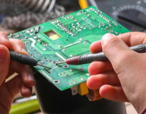
Time-Domain Reflectometry (TDR) is widely used for evaluating transmission-line impedance and identifying local discontinuities.
During TDR testing, engineers should examine the complete impedance profile rather than relying solely on a single average value. A relatively stable waveform generally indicates a more uniform transmission-line structure, while sharp peaks, drops, steps, or localized deviations may indicate structural discontinuities.
Potential sources include:
- Via transitions
- Connector or test-launch structures
- Trace-width variation
- Layer transitions
- Differential-pair spacing changes
- Reference-plane discontinuities
- Local copper geometry changes
- Improper test-fixture compensation
However, a waveform deviation should not automatically be classified as a PCB defect. The engineer should first determine whether the deviation originates from the PCB itself, the test fixture, the probe, the launch structure, or measurement setup.
Test-system parasitics and fixture characteristics should therefore be properly characterized and, where appropriate, de-embedded or compensated before interpreting the effective PCB impedance.
Frequency-Appropriate Verification
High-speed interfaces may operate over a wide range of frequency components. For interfaces such as 10 Gb/s, 25 Gb/s, and higher-speed serial links, the relevant signal spectrum depends on the data rate, rise/fall time, encoding, channel structure, and transmitter/receiver characteristics.
Therefore, impedance verification should be correlated with the actual application rather than assuming that a single low-frequency measurement fully represents high-speed system behavior.
Engineers should consider:
- Actual interface data rate
- Signal rise and fall time
- PCB material Dk and Df
- Trace geometry
- Copper roughness
- Layer stackup
- Via structure
- Required insertion loss
- Return loss and reflection behavior
For demanding high-frequency designs, material characterization and electromagnetic simulation can provide additional information beyond conventional impedance measurements.
3. Differential Impedance Requires Dedicated Control
Differential signaling is widely used in high-speed interfaces because it can provide improved noise immunity and support high data rates. However, the performance of a differential pair depends on more than its nominal differential impedance.
During differential impedance verification, engineers should examine:
- Differential impedance
- Single-ended impedance
- Trace width
- Trace spacing
- Pair-to-pair coupling
- Length matching where required
- Reference-plane continuity
- Via transitions
- Local geometry variation
Maintaining consistent spacing between the two traces is particularly important because changes in coupling affect differential impedance.
A localized increase or decrease in spacing can therefore create a corresponding impedance variation.
At the same time, differential pairs should maintain an appropriate return-current environment. Removing nearby copper or adding unnecessary structures around the pair can change the electromagnetic environment and affect the transmission characteristics.
For high-speed differential channels, impedance control should therefore be performed together with routing and reference-plane analysis rather than treated as an isolated PCB parameter.
4. Common Causes of High-Speed Impedance Discontinuities
Several physical features commonly contribute to impedance discontinuities.
Trace Geometry Variation
Changes in trace width or spacing can modify the characteristic impedance. Etching uniformity, over-etching, under-etching, and manufacturing tolerances should therefore be controlled.
Layer Transitions
Whenever a high-speed signal changes layers, its via structure and reference-plane relationship change. The transition can introduce additional inductance, capacitance, and electromagnetic discontinuity.
Via geometry, pad size, anti-pad dimensions, stub length, and reference-via placement should therefore be considered during high-speed design.
Reference-Plane Discontinuity
A transmission line depends on its surrounding electromagnetic environment. Plane splits, voids, inappropriate copper clearances, and changes in reference layers can disturb the return-current path.
A signal trace crossing a reference-plane discontinuity may therefore experience additional reflection or electromagnetic coupling.
Copper Surface Roughness
At high frequencies, conductor surface roughness can increase conductor loss because high-frequency current tends to concentrate near the conductor surface.
Therefore, high-frequency PCB material selection should consider copper profile and surface roughness together with dielectric properties and trace geometry.
5. Optimization Strategies for Impedance Retest Failures
When impedance retesting identifies a local discontinuity, the first step should be to determine the physical source rather than immediately changing the target impedance.
For trace-related issues, engineers can review:
- Trace width
- Differential spacing
- Copper thickness
- Etching compensation
- Dielectric thickness
- Reference-plane distance
For via-related issues, optimization may include:
- Via pad dimensions
- Anti-pad geometry
- Via diameter
- Stub length
- Back-drilling requirements
- Reference-via arrangement
For stackup-related problems, engineers should review the actual dielectric thickness, material Dk/Df values, copper thickness, and manufacturing tolerances.
If the selected laminate cannot provide the required loss or electrical performance, a lower-loss, high-frequency material may need to be considered.
Material replacement should be based on the complete channel requirement rather than impedance alone.
6. Verification Should Combine TDR, Simulation, and Physical Testing
A reliable signal integrity verification strategy normally combines multiple methods.
TDR testing is useful for identifying localized impedance discontinuities and checking transmission-line uniformity.
Electromagnetic simulation can help evaluate the influence of trace geometry, vias, stackup, materials, and other structures before fabrication.
S-parameter measurements can provide information about insertion loss, return loss, and channel transmission characteristics when appropriate test equipment and fixtures are available.
For particularly demanding applications, engineers may also perform eye-diagram testing, bit-error-rate testing, or complete channel compliance testing at the system level.
Each method answers a different question. Therefore, no single measurement should be treated as a universal replacement for all other forms of verification.
7. Control Manufacturing Variables During Mass Production
Maintaining stable impedance during mass production requires more than testing finished boards.
Manufacturers should control the manufacturing variables that directly influence transmission-line geometry and dielectric structure.
Important parameters include:
- PCB stackup consistency
- Dielectric thickness
- Copper thickness
- Trace width
- Etching uniformity
- Copper roughness
- Laminate batch consistency
- Plating thickness
- Registration accuracy
- Via geometry
Process capability should be monitored over production batches to identify systematic drift.
If impedance gradually moves toward the specification limit, corrective action can be taken before large quantities of boards become nonconforming.
This process-oriented approach is generally more effective than relying solely on final-product inspection.
8. Establish a Traceable High-Speed Impedance Retest Procedure
For high-speed multilayer PCBs, a standardized verification workflow can improve both reliability and traceability.
Step 1: Confirm the Design Target
Define single-ended and differential impedance requirements based on the interface specification and system design.
Step 2: Verify the Stackup
Confirm dielectric thickness, material properties, copper thickness, and reference-plane relationships.
Step 3: Select Representative Test Structures
Use impedance coupons or suitable test structures that represent the actual production stackup and critical transmission-line geometry.
Step 4: Perform TDR Measurement
Measure the impedance profile and identify localized discontinuities.
Step 5: Investigate Abnormal Regions
Check vias, layer transitions, trace geometry, reference planes, and test structures.
Step 6: Perform Additional High-Frequency Verification
Where required, supplement TDR with S-parameter measurements, simulation, or system-level channel testing.
Step 7: Maintain Production Traceability
Record test conditions, equipment settings, calibration status, material batches, stackup information, and test results.
This makes it easier to distinguish design-related problems from manufacturing variation.
9. Avoid Over-Interpreting a Single Impedance Measurement
One of the most important principles in high-speed PCB impedance testing is that a passing impedance number does not automatically guarantee successful high-speed system operation.
System-level performance depends on the complete signal channel, including:
- Transmitter
- PCB traces
- Vias
- Connectors
- Packages
- Receiver
- Reference planes
- Power integrity
- Loss and reflection characteristics
A PCB may meet its impedance specification but still produce unacceptable channel loss or timing margins at the system level.
Conversely, a small TDR deviation does not necessarily mean that the entire channel will fail.
The appropriate acceptance criteria should therefore be based on the interface specification, PCB fabrication capability, channel simulation, and actual system requirements.
Conclusion
High-speed multilayer PCB impedance verification requires more than checking whether a measured value falls within a predefined tolerance.
A comprehensive approach should combine PCB impedance control, TDR testing, differential impedance verification, stackup management, material characterization, manufacturing-process control, and system-level signal integrity analysis.
For 5G communication equipment, high-speed servers, AI hardware, and other demanding electronic systems, engineers should pay particular attention to local impedance discontinuities, reference-plane continuity, via transitions, copper roughness, dielectric properties, and manufacturing variation.
By establishing a traceable and application-specific impedance verification process, manufacturers can identify potential transmission-channel problems earlier and improve the consistency of high-speed PCB production.
Kingda can support high-speed and multilayer PCB projects with impedance-controlled fabrication, stackup verification, impedance testing, manufacturing-process monitoring, and reliability-oriented quality control to help customers achieve stable high-speed signal transmission.