As PCB operating frequencies continue to increase, material stability becomes increasingly important. This is especially true for 6G PCB designs, millimeter-wave radar, high-speed communication equipment, and other RF applications where even small changes in dielectric properties can affect impedance, phase, insertion loss, and overall system performance.
After reflow or other thermal processes, engineers may sometimes observe unexpected changes in S-parameters, insertion loss, or phase response. One possible cause is moisture absorption in the PCB dielectric material.
Moisture does not simply act as an additional contaminant. Water molecules can interact with the polymer network and alter the effective electromagnetic properties of the laminate. As moisture content increases, the effective dielectric constant and dissipation factor may change, while thermal exposure can further influence resin structure and dimensional stability.
The actual magnitude of these changes depends on laminate chemistry, frequency, temperature, moisture content, glass/resin distribution, and measurement method. Therefore, moisture-related electrical drift should be evaluated using material-specific data rather than a single universal threshold.
How Moisture Changes PCB Dielectric Properties
Many conventional FR-4 materials contain epoxy resin systems with polar chemical groups. These groups can interact with absorbed water through hydrogen bonding and other molecular interactions.
Once water enters the polymer network, several effects can occur simultaneously.
First, water changes the local dielectric environment of the resin. Because water has a strong frequency-dependent dielectric response, absorbed moisture can increase the effective dielectric constant of the composite material.
Second, water molecules introduce additional dielectric relaxation mechanisms. Under an alternating electromagnetic field, molecular polarization and relaxation can contribute to dielectric loss.
As a result, both Dk and Df may shift as moisture content changes.
However, the relationship is not necessarily linear. The response depends on how water is distributed within the resin, glass fibers, interfaces, and microscopic free volume.
This means that two PCB materials with the same nominal Dk under dry conditions may exhibit significantly different electrical stability after humidity exposure.
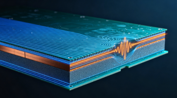
Moisture Absorption Can Affect High-Frequency Performance
The impact becomes more important as operating frequency increases.
For a controlled-impedance transmission line, impedance depends on the physical geometry and the effective dielectric properties surrounding the conductor. A simplified relationship can be represented as:
[Z_0=f(W,T,H,D_k)]
where:
- W is trace width
- T is copper thickness
- H is the distance to the reference plane
- Dk is the effective dielectric constant
If moisture changes the effective Dk, the characteristic impedance can shift even though the copper geometry remains unchanged.
For RF and millimeter-wave circuits, this can affect:
- Insertion loss
- Phase delay
- Return loss
- Impedance matching
- Group delay
- Antenna performance
- Filter response
- Calibration stability
Therefore, moisture control is not only a material-storage issue. It can become a signal integrity and RF performance issue.
Dk and Df Do Not Change in the Same Way
Dk primarily describes the dielectric constant and determines how electromagnetic energy propagates through the dielectric environment.
Df, or dissipation factor, describes dielectric loss.
Moisture can influence both parameters, but the mechanisms and sensitivity may differ.
At higher frequencies, dielectric loss can become particularly important because the total channel loss includes contributions from both dielectric and conductor losses.
A simplified relationship can be expressed conceptually as:
[Loss_{total}=Loss_{dielectric}+Loss_{conductor}+Loss_{via}+Loss_{connector}+\cdots]
Therefore, an increase in Df does not automatically explain the entire increase in insertion loss. Engineers should also evaluate copper roughness, trace length, conductor geometry, vias, connectors, surface finish, and impedance discontinuities.
Moisture Effects May Become Nonlinear
It is tempting to define one moisture percentage as the universal point at which Dk or Df suddenly changes. In practice, this is rarely reliable across different PCB materials.
Moisture uptake depends on:
- Resin chemistry
- Resin content
- Glass style
- Laminate construction
- Temperature
- Relative humidity
- Exposure time
- Surface condition
- Board thickness
- Material curing state
At low moisture levels, absorbed water may be distributed within the polymer network without producing a dramatic electrical change.
As moisture increases, water may preferentially accumulate around resin-rich regions or material interfaces. The effective dielectric response can then become increasingly nonlinear.
For this reason, a moisture-versus-Dk/Df characterization curve is more useful than applying a single universal “critical” moisture value.
Why 6G and Millimeter-Wave PCBs Are More Sensitive
For a 6G PCB or millimeter-wave radar board, the wavelength is much shorter than in conventional digital systems.
At these frequencies, relatively small variations in:
- Dielectric thickness
- Dk
- Df
- Trace width
- Copper roughness
- Surface finish
- Via geometry
- Material moisture
can produce measurable changes in electrical performance.
This does not mean that every conventional FR-4 material is unsuitable for high-frequency applications. Instead, material selection should be based on the required frequency, channel length, loss budget, environmental conditions, and manufacturing capability.
For some lower-frequency or short-distance applications, a suitable low-loss FR-4 system may provide adequate performance. For demanding millimeter-wave applications, materials with lower moisture sensitivity and tighter dielectric-property control may be more appropriate.
High-Frequency PCB Material Selection
When selecting high-frequency PCB materials, engineers should look beyond the nominal Dk value.
Important parameters include:
- Dk and Df at the target frequency
- Dk tolerance
- Moisture absorption
- Temperature coefficient of Dk
- Resin system
- Glass-weave structure
- Copper foil roughness
- Thermal stability
- Dimensional stability
- CTE
- Processing compatibility
The test method is also important. Dk values obtained using different test frequencies, sample structures, resin contents, or measurement techniques should not be compared directly without understanding the methodology.
For RF and millimeter-wave designs, material suppliers should ideally provide dielectric-property data over the frequency and temperature range relevant to the actual application.
Moisture and the Glass-Weave Effect
Glass-reinforced laminates are heterogeneous materials rather than uniform dielectric blocks.
The glass fibers and resin have different dielectric properties. When moisture is absorbed, the local dielectric environment can therefore change differently in resin-rich and glass-rich regions.
This can contribute to local variation in effective Dk and influence high-speed propagation.
For tightly controlled RF structures, engineers should consider:
- Trace orientation relative to the glass weave
- Glass style
- Resin content
- Dielectric thickness
- Local copper geometry
- Moisture condition
This is particularly important when designing long RF transmission lines or circuits operating at millimeter-wave frequencies.
Moisture Can Also Affect PCB Reliability
The electrical effects of moisture are only part of the problem.
Moisture can also influence:
- Lamination quality
- Interfacial adhesion
- Reflow behavior
- Delamination resistance
- Dimensional stability
- CAF-related reliability
- Soldering performance
- Long-term insulation resistance
During thermal processing, trapped moisture may rapidly expand into vapor. If the material has insufficient resistance to moisture-related degradation, the resulting internal pressure can contribute to delamination or other structural defects.
Therefore, moisture control should be considered as part of overall PCB reliability, not only RF performance.
Common Mistakes in Moisture Management
Mistake 1: Assuming baking always solves the problem
Baking can remove absorbed moisture, but the correct temperature and duration depend on the laminate, board construction, moisture level, and subsequent assembly process.
Excessive baking may also introduce oxidation, material aging, or other process issues. The recommended conditioning procedure should therefore follow the material supplier’s specifications and the applicable assembly requirements.
Mistake 2: Confusing moisture absorption with water content
Moisture absorption is normally expressed as a change in mass under a defined conditioning procedure. It should not be confused with a simple volumetric percentage of water inside the board.
The test method, specimen preparation, conditioning environment, and measurement procedure must be clearly defined before comparing results.
Mistake 3: Using one moisture threshold for every material
A single value such as 0.8%, 1.0%, or 1.5% should not automatically be treated as a universal acceptance criterion.
Different resin systems can exhibit different moisture sensitivity and dielectric-property drift.
Mistake 4: Looking only at room-temperature Dk
For RF and millimeter-wave applications, Dk should be evaluated at the actual operating frequency and relevant temperature and humidity conditions.
A Practical Validation Process
For a new PCB materials system, a practical validation process can be divided into four stages.
Step 1: Establish baseline material data
Record:
- Dk
- Df
- Moisture absorption
- Tg
- Td
- CTE
- Copper roughness compatibility
- Dimensional stability
The measurement frequency and test method should be recorded with the values.
Step 2: Perform controlled humidity conditioning
Condition representative material or PCB samples under defined temperature and relative-humidity conditions.
After conditioning, measure moisture uptake and repeat the dielectric-property measurements.
This produces a material-specific relationship between moisture level and Dk/Df.
Step 3: Test the actual PCB structure
Material-level measurements alone may not reproduce the behavior of the final PCB.
The finished board should be evaluated through:
- TDR impedance testing
- S-parameter measurement
- Insertion-loss testing
- Phase or group-delay measurement
- Cross-sectional inspection
- Dimensional measurement
For millimeter-wave designs, calibrated fixtures and appropriate de-embedding methods are particularly important.
Step 4: Validate after assembly exposure
If the PCB will undergo reflow, wave soldering, multiple thermal cycles, or other high-temperature processes, testing should include representative assembly conditions.
Compare the electrical performance before and after exposure.
This helps determine whether the observed drift originates from moisture, thermal history, material curing, structural deformation, or another process variable.
PCB Storage and Handling Recommendations
Moisture management should begin before assembly.
A practical control process includes:
- Store moisture-sensitive materials according to supplier requirements.
- Keep unused PCB panels in appropriate moisture-barrier packaging.
- Use desiccant or humidity-control measures where specified.
- Minimize uncontrolled exposure after opening the package.
- Record opening time and environmental conditions for sensitive materials.
- Apply controlled preconditioning or baking when required.
- Re-seal unused boards after production.
- Use representative moisture checks for high-reliability programs.
For high-frequency boards, storage controls should be linked to electrical validation rather than based only on visual inspection.

Kingda’s Approach to High-Frequency PCB Materials
At Kingda, material selection for high-frequency PCB manufacturing can be evaluated from both electrical and manufacturing perspectives.
For demanding RF, high-speed, and 6G PCB applications, the evaluation can include Dk/Df stability, moisture sensitivity, stackup construction, copper roughness, impedance control, thermal behavior, and manufacturing compatibility.
The objective is not simply to choose a material with the lowest nominal Dk or Df. The material must remain sufficiently stable across the actual frequency, temperature, humidity, assembly process, and lifetime requirements of the product.
By combining material characterization, controlled moisture conditioning, stackup analysis, prototype fabrication, and electrical validation, engineers can identify moisture-related risks before they become production or field failures.
Conclusion
Moisture absorption can change the effective dielectric properties of PCB materials and influence Dk, Df, impedance, insertion loss, phase stability, and long-term reliability.
The effect is especially important for high-frequency PCB, RF, and millimeter-wave applications, where small electrical variations can become significant at the system level.
Rather than relying on a universal moisture threshold, engineers should evaluate material-specific moisture behavior, dielectric-property stability, environmental conditions, and actual PCB construction.
For advanced RF and 6G PCB designs, controlling moisture from material storage through assembly and final validation is an important part of achieving stable and repeatable electrical performance.