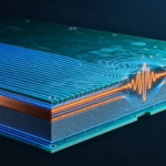
In high-density PCB assemblies, removing copper beneath a BGA package is sometimes considered a way to improve solder-joint reliability or provide more routing space. However, copper removal does not automatically improve thermal performance.
In many cases, the result depends on where the copper is removed, which layers are affected, and whether the copper removal interferes with the main thermal path.
This is particularly important for power-management ICs, processors, RF devices, 5G equipment, and other high-density assemblies where BGA packages must transfer heat efficiently into the PCB.
The key principle of BGA thermal management is simple: thermal energy should be directed through the lowest-resistance available path rather than blocked by unnecessary copper-plane removal.
Copper Voiding Does Not Automatically Improve Thermal Performance
Copper has a much higher thermal conductivity than conventional FR-4 dielectric material. Therefore, copper planes and copper-filled structures can provide effective lateral heat-spreading paths inside a PCB.
A simplified thermal path may look like:
Die → Package → BGA structure → PCB copper → Thermal vias → Internal copper planes → Heat spreader or chassis
If copper is removed from a region that is not part of the main heat-transfer path, the effect may be small.
However, if the void extends across the region containing the primary thermal vias, copper planes, or heat-spreading structures, the thermal path can become longer or more resistive.
The result can be increased thermal resistance and higher component temperature.
Therefore, copper-plane removal should be evaluated together with the complete thermal structure rather than treated as an isolated layout operation.

Thermal Vias Are Often More Important Than Copper Voiding
For many BGA thermal designs, thermal vias provide the critical vertical connection between the package area and internal copper planes.
A thermal via transfers heat from the surface region toward internal copper layers and, depending on the PCB structure, can eventually connect to a backside heat spreader or mechanical cooling structure.
The effectiveness of this path depends on:
- Via diameter
- Via barrel copper thickness
- Via density
- Via pitch
- Number of vias
- Connection to internal copper planes
- Pad geometry
- Board thickness
- Copper thickness
- Thermal interface conditions
A common design mistake is to create a large copper void under the BGA and unintentionally remove the copper surrounding the thermal-via array.
This can reduce the effectiveness of the intended heat-transfer network.
A better strategy is to distinguish between electrical clearance zones and thermal conduction zones. Copper should be removed only where required for electrical, manufacturing, or mechanical reasons while preserving the copper structures that contribute to heat spreading.
Why Layer-by-Layer Copper Distribution Matters
A multilayer PCB does not behave as a single homogeneous thermal block.
Each copper layer contributes differently depending on its copper thickness, area, connectivity, and relationship to the thermal-via structure.
For example, a BGA package may have:
- Surface copper for local heat spreading
- An internal ground plane
- An internal power or thermal plane
- Multiple thermal-via connections
- A backside copper region
- A mechanical heat-spreading interface
Removing copper from one layer does not necessarily produce the same result as removing it from every layer.
This is why PCB stackup should be considered during BGA thermal optimization.
A designer may choose to create electrical clearance on one internal layer while maintaining a continuous copper region on another layer to preserve the thermal path.
The actual optimum depends on the package construction, signal routing, power distribution, via structure, and cooling method.
BGA Pad Clearance and Thermal Vias Must Be Designed Together
The area immediately beneath a BGA contains multiple competing requirements.
The design may need to accommodate:
- Solder pads
- Escape routing
- Thermal vias
- Ground vias
- Power vias
- Anti-pads
- Copper planes
- Solder-mask structures
If these elements are designed independently, one optimization can easily damage another.
For example, increasing a plane clearance may provide additional electrical isolation but simultaneously remove copper that was helping to spread heat.
Likewise, placing thermal vias too close to solder pads can introduce solder-wicking or assembly concerns if the via structure is not properly designed and filled or capped where required.
Therefore, the thermal-via array, BGA footprint, solder-mask design, and internal copper planes should be reviewed as one system.
Copper Plane Design and Thermal Resistance
Thermal performance can be understood through the concept of thermal resistance:
[R_{\theta}=\frac{\Delta T}{P}]
where:
- (R_{\theta}) is thermal resistance
- (\Delta T) is the temperature difference
- (P) is the dissipated power
The lower the thermal resistance, the more effectively heat can be transferred away from the component.
Copper-plane removal can increase thermal resistance if it reduces the effective heat-spreading area or interrupts a low-resistance path.
However, simply increasing copper area does not guarantee proportional thermal improvement. Heat transfer also depends on:
- Copper thickness
- Copper area
- Via configuration
- Board thickness
- Thermal interfaces
- Airflow
- Heat sink structure
- Component power dissipation
- Enclosure design
For this reason, PCB thermal performance should be evaluated at the system level.
Thermal Design Must Be Balanced With Signal Integrity
BGA copper optimization is not purely a thermal problem.
Modern BGA packages often contain high-speed interfaces, power-distribution networks, and sensitive analog or RF signals.
A continuous copper plane may provide an excellent thermal path but create unwanted electrical coupling if it is used without considering signal integrity.
Conversely, excessive copper removal can damage the return path of high-speed signals.
The design therefore needs to balance:
- Thermal conduction
- Power integrity
- Signal integrity
- EMI/EMC performance
- Electrical clearance
- Routing density
- Manufacturing capability
For high-speed BGA devices, engineers should avoid treating thermal copper and reference-plane copper as completely independent structures.
Copper Plane Voiding Around BGA Regions
A useful design strategy is to divide the BGA region into functional zones.
Zone 1: Solder-joint region
The copper structure must comply with the selected pad design and assembly process. Excessive copper imbalance should be avoided because it can influence solder-joint behavior and thermal distribution.
Zone 2: Thermal-via region
This region should preserve an efficient vertical heat-transfer path. Thermal vias should connect to appropriate internal copper structures.
Zone 3: High-speed signal region
Signals that require controlled impedance should maintain an appropriate reference plane and return path.
Zone 4: Power-distribution region
Power and ground structures should be designed to minimize both electrical impedance and unwanted thermal bottlenecks.
This functional approach is generally more reliable than applying a single “void everything under the BGA” rule.
The Effect of Dielectric Thickness
The distance between copper layers also influences both electrical and thermal behavior.
A thicker dielectric can increase the vertical distance between copper planes, while a thinner dielectric can strengthen electromagnetic coupling between adjacent planes.
From a thermal perspective, the dielectric itself is relatively resistive compared with copper. Therefore, designers often rely on copper planes and plated vias to provide efficient lateral and vertical heat-transfer paths.
However, changing dielectric thickness also changes impedance, capacitance, layer spacing, board thickness, and mechanical behavior.
Consequently, dielectric thickness should not be optimized solely for thermal performance.
CTE Mismatch and BGA Solder-Joint Reliability
BGA thermal design must also consider mechanical reliability.
During reflow and operating-temperature cycling, the PCB laminate, copper, package substrate, and solder joints expand at different rates.
This CTE mismatch can produce cyclic mechanical strain in the solder joints.
Copper removal may alter local stiffness and thermal distribution, but the effect is highly dependent on board construction and package geometry.
The relationship between copper-plane design and solder-joint fatigue is therefore not a simple “more copper is better” or “less copper is better” rule.
Engineers should consider:
- PCB thickness
- Copper distribution
- Package size
- BGA pitch
- Solder alloy
- Board material
- Thermal cycling range
- Component location
- Mechanical constraints
For demanding products, thermal and mechanical simulations should be supported by physical reliability testing.
Three Common BGA Thermal Design Failures
Failure 1: Removing the entire internal copper region
A large copper void may unintentionally remove the heat-spreading path connected to the thermal-via array.
The result can be higher junction temperature even though the designer intended only to improve electrical clearance.
Failure 2: Removing copper around thermal vias
Thermal vias need an effective copper connection to transfer heat. If the surrounding plane is removed without considering the via connection, the vertical thermal path can become less effective.
Failure 3: Reviewing only one PCB layer
A thermal path can pass through several layers. Removing copper from one layer may have little effect, while removing it from several connected layers can significantly change the total thermal resistance.
Therefore, the entire cross-sectional structure should be reviewed.
A Practical Three-Step Evaluation Method
Instead of relying on a fixed copper-clearance rule, engineers can use a three-step evaluation process.
Step 1: Map the thermal path
Identify the complete path from the BGA die or package thermal interface to the final heat sink, chassis, or ambient environment.
Mark every copper plane, via array, thermal pad, and interface along the path.
Step 2: Compare copper-void configurations
Evaluate several candidate structures, such as:
- Continuous copper
- Localized copper clearance
- Single-layer copper removal
- Multilayer copper removal
- Copper removal with preserved thermal-via regions
Compare the thermal resistance and electrical performance of each structure.
Step 3: Validate with hardware
Use thermal simulation as an engineering tool, then verify the final design through physical measurements.
Useful validation methods include:
- Infrared thermal imaging
- Thermocouple measurements
- Junction-temperature estimation
- Full-load testing
- Transient-load testing
- Thermal cycling
- Cross-sectional inspection
The measurement setup should account for emissivity, package surface conditions, airflow, fixture effects, and ambient temperature.

CAM and DFM Review Before Manufacturing
Before releasing the design to PCB manufacturing, the CAM and DFM review should verify the relationship between BGA pads, thermal vias, copper planes, and internal clearances.
A practical checklist includes:
- Identify every BGA package requiring thermal management.
- Locate the thermal-via array.
- Determine which internal copper layers are part of the thermal path.
- Check whether plane voids interrupt those connections.
- Review via-pad and anti-pad structures.
- Check solder-mask and via-fill requirements.
- Review high-speed signal reference planes.
- Verify copper balance around the BGA.
- Run thermal and electrical simulations where necessary.
- Validate the prototype under representative load conditions.
This process can prevent a common mistake: optimizing one layer for routing while unintentionally creating a thermal bottleneck in another layer.
Kingda’s Approach to BGA Thermal Design
At Kingda, BGA layout and PCB thermal design can be evaluated together with stackup planning, thermal-via structures, copper distribution, signal integrity, and DFM requirements.
The goal is not simply to remove copper beneath a BGA. Instead, the copper structure should be intentionally designed so that electrical clearance, thermal conduction, mechanical reliability, and manufacturability work together.
For high-power and high-density BGA applications, preserving the correct thermal-via and copper-plane network is often more important than maximizing the size of a copper-free region.
The fundamental principle is straightforward:
Copper should be removed only where it is necessary. Thermal vias and their copper connections should remain part of a continuous, low-resistance heat-transfer path whenever the PCB architecture requires them.
With proper BGA thermal management, optimized thermal vias, and a carefully designed PCB stackup, engineers can achieve better thermal stability without unnecessarily sacrificing signal integrity or manufacturing reliability.