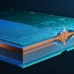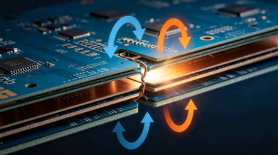
Microcracks formed during PCB lamination may remain invisible immediately after manufacturing but gradually develop under repeated thermal cycling. This is particularly important for multilayer PCBs with BGA packages, where differences in thermal expansion between copper, laminate, prepreg, and package structures can create repeated mechanical loading.
For example, after thermal cycling between low and high temperatures, cross-sectional analysis may reveal radial microcracks near BGA pad structures or within the prepreg layer even though no obvious delamination was detected during the initial inspection.
This type of failure should not automatically be attributed to residual stress from lamination alone. In many cases, the interaction between CTE mismatch, material properties, copper geometry, lamination history, and repeated temperature changes determines whether an initial micro-defect remains stable or develops into a reliability concern.
The Core Mechanism: CTE Mismatch and Interfacial Fatigue
The most important mechanism is the repeated strain generated by differences in the coefficient of thermal expansion between different PCB materials.
Copper has a relatively low CTE compared with the Z-axis expansion of many conventional FR-4 structures, particularly above the glass-transition region. During thermal cycling, the laminate and copper therefore expand and contract at different rates.
This mismatch can generate mechanical stress at:
- Copper-to-dielectric interfaces
- Prepreg-to-core interfaces
- Via structures
- BGA pad regions
- Resin-rich or glass-weave regions
- Areas with abrupt copper-density changes
The temperature excursion itself does not determine the resulting stress. The actual response also depends on elastic modulus, viscoelastic behavior, layer thickness, copper pattern geometry, temperature dwell time, heating/cooling rate, and the degree of mechanical constraint.
A simplified relationship can be expressed as:
[\epsilon_{thermal} \approx \Delta CTE \times \Delta T]
This equation provides an intuitive way to understand why a larger CTE difference or temperature excursion can increase thermally induced strain. However, it should not be used by itself to predict actual interface stress or crack growth.
Why Microcracks Can Grow After Manufacturing
A key characteristic of PCB microcracks is that they may not become immediately visible after lamination.
Small defects can exist around resin-rich areas, glass bundles, copper edges, drilled features, or interfaces. During subsequent thermal cycles, these locations experience repeated mechanical loading.
The process can be viewed as:
- A microscopic defect or weak interface exists.
- Thermal expansion creates cyclic strain.
- Local stress concentrates around the defect.
- Repeated cycling causes crack-tip damage.
- The crack gradually propagates along an interface or through the dielectric.
- The defect eventually becomes large enough to affect electrical or mechanical reliability.
Therefore, a board that passes an initial visual inspection may still require reliability testing if its application involves significant thermal cycling.
Dk and Df Changes Should Be Evaluated Carefully
The original electrical properties of a laminate are also affected by its resin chemistry, glass structure, moisture content, temperature, and curing state.
Dk and Df are important for high-speed electrical performance, but they should not be treated as direct predictors of mechanical crack growth.
During lamination and subsequent thermal exposure, resin curing, moisture desorption, and temperature-dependent dielectric behavior can change the effective electrical properties of the material.
However, a change in Dk or Df does not automatically mean that mechanical reliability has degraded. Electrical-property measurements should therefore be correlated with:
- Resin cure state
- Glass/resin distribution
- Moisture absorption
- Z-axis CTE
- Modulus versus temperature
- Thermal decomposition behavior
- Interfacial adhesion
- Cross-sectional morphology
For high-speed multilayer PCBs, electrical and mechanical material characterization should be evaluated together rather than using Dk/Df alone.
Z-Axis CTE Is an Important Material Selection Parameter
For multilayer structures, Z-axis expansion deserves particular attention because it represents dimensional changes through the thickness of the PCB.
Instead of selecting material only by Tg, engineers should evaluate the complete temperature-dependent behavior of the laminate, including:
- Z-axis CTE
- Tg
- Decomposition temperature (Td)
- Modulus above Tg
- Resin content
- Cure characteristics
- Moisture resistance
- Interlaminar adhesion
A lower Z-axis CTE can reduce thermally induced dimensional changes in some multilayer structures, but it is not automatically the best solution for every application.
Material selection should consider the entire construction, including core, prepreg, copper thickness, via structures, BGA package dimensions, and expected operating temperature.
Copper Geometry Can Concentrate Stress
Copper distribution is another important factor in lamination reliability.
Large changes in copper thickness or copper density can produce local differences in mechanical constraint and resin flow. For example, an abrupt transition from thin copper to much thicker copper can create a localized region where the dielectric and copper respond differently during thermal processing.
Engineers should therefore review:
- Copper thickness transitions
- Large copper pours
- Plane openings
- Dense BGA regions
- Via fields
- Thermal pads
- Copper-free areas
- High-density and low-density regions
Balanced copper distribution can help improve lamination consistency and reduce local mechanical variation.
BGA Structures Require Additional Attention
BGA packages are particularly sensitive to PCB mechanical behavior because their solder joints connect a relatively rigid package structure to a multilayer PCB.
During temperature changes, the package, solder joints, PCB laminate, and copper structures may expand differently.
This can produce cyclic deformation in the solder joints and surrounding PCB structure.
When a microcrack exists near a BGA pad or dielectric interface, the additional mechanical loading may accelerate crack propagation.
However, BGA reliability is not controlled by PCB CTE alone. Package size, solder alloy, pad design, board thickness, component placement, assembly profile, underfill, and system-level constraints can all influence solder-joint fatigue.
Thermal Cycling Rate Also Matters
Thermal cycling should not be evaluated only by minimum and maximum temperatures.
Important parameters include:
- Temperature range
- Ramp rate
- Dwell time
- Number of cycles
- Chamber recovery time
- Specimen configuration
- Board thickness
- Component package size
A very rapid temperature transition can create transient temperature gradients between different layers and components. Conversely, longer dwell periods allow materials to approach thermal equilibrium but may introduce additional time-dependent effects.
Therefore, test conditions should be selected according to the applicable product specification, reliability standard, and actual application environment.
Common Material Selection Mistakes
Several common approaches can lead to incorrect conclusions about lamination reliability.
Mistake 1: Selecting material by Tg alone
A high Tg does not automatically guarantee low thermal stress or superior BGA reliability. Z-axis CTE, modulus, cure behavior, and interfacial adhesion also need to be considered.
Mistake 2: Treating one Z-axis CTE value as universal
CTE can change significantly with temperature, especially around and above Tg. The measurement method and temperature range should therefore be reviewed before comparing materials.
Mistake 3: Using Dk/Df as mechanical reliability indicators
Dk and Df are primarily electrical material parameters. They should be correlated with mechanical and thermal data rather than used as direct indicators of crack resistance.
Mistake 4: Ignoring copper distribution
Even when the laminate itself meets its specification, severe copper-density variation can influence resin flow, local stress, and final board geometry.
Mistake 5: Assuming X-ray inspection can identify every microcrack
X-ray inspection is useful for many PCB and assembly defects, but very small dielectric or interfacial cracks may require cross-sectioning, microscopy, or other failure-analysis techniques.
A Practical Validation Process for New Prepreg Materials
When introducing a new PCB laminate or prepreg system, a structured validation process is more reliable than applying a single pass/fail number.
Step 1: Characterize the material
Review or measure:
- Z-axis CTE
- Tg
- Td
- Modulus versus temperature
- Dk and Df
- Moisture absorption
- Resin content
- Cure characteristics
TMA can be useful for characterizing temperature-dependent dimensional behavior, but the test range and methodology should match the intended application.
Step 2: Build representative test coupons
The coupon should reproduce the actual production structure as closely as possible, including:
- Core and prepreg selection
- Copper thickness
- Copper density
- Via structures
- Pad geometry
- Relevant layer transitions
Testing an isolated material coupon may not reproduce the stress conditions of a production multilayer board.
Step 3: Perform thermal cycling
Use the temperature range and cycle count defined by the applicable reliability requirement. After cycling, inspect the critical interfaces using cross-sections and microscopy.
Look for:
- Interfacial cracks
- Resin cracking
- Glass/resin separation
- Pad-interface damage
- Via-related defects
- Delamination
- Crack propagation
Step 4: Correlate physical and electrical results
For high-speed products, compare structural inspection with electrical measurements. Changes in impedance, insertion loss, resistance, or leakage can provide additional evidence of material or structural degradation.
Failure Analysis Should Focus on Crack Origin
When a crack is discovered, simply measuring its final length is not enough.
A useful failure-analysis workflow should determine:
- Where the crack initiated.
- Which material or interface it followed.
- Whether it propagated through resin, along glass/resin boundaries, or along a copper interface.
- Whether copper geometry contributed to stress concentration.
- Whether moisture or thermal history accelerated the damage.
- Whether the defect originated during fabrication or developed during reliability testing.
Cross-sectional microscopy is often the first step. Additional analytical methods such as SEM, elemental analysis, or material characterization can be used when the failure mechanism remains uncertain.
This approach helps distinguish a manufacturing defect from a reliability-driven crack-growth mechanism.
How to Reduce Lamination Microcrack Risk
A practical prevention strategy should combine material, stackup, process, and reliability controls.
Optimize material selection:
Evaluate Z-axis CTE, Tg, Td, modulus, cure behavior, moisture resistance, and interfacial adhesion together.
Improve stackup consistency:
Use a realistic pressed stackup rather than relying only on nominal prepreg thickness.
Control copper distribution:
Avoid abrupt copper-density and copper-thickness transitions around mechanically sensitive regions.
Optimize lamination parameters:
Control temperature profile, pressure, heating rate, resin flow, and cooling conditions according to the material supplier’s process window.
Control moisture:
Moisture can influence dielectric behavior, delamination resistance, and thermal stress. Storage and preconditioning should follow the applicable material and assembly requirements.
Validate with representative testing:
Thermal cycling, cross-section inspection, warpage measurement, and electrical verification should be combined when the product has demanding reliability requirements.
Kingda’s Approach to PCB Reliability
At Kingda, material selection and multilayer PCB manufacturing can be evaluated as an integrated engineering process rather than as isolated parameters.
For BGA and high-density multilayer designs, the review can include stackup construction, prepreg selection, copper distribution, lamination conditions, thermal behavior, and reliability validation.
The objective is not simply to select the lowest CTE material. The complete material-structure-process combination must be compatible with the PCB’s operating temperature, package structure, electrical requirements, and manufacturing process.
By identifying potential weak interfaces before mass production and validating them through representative thermal cycling and failure analysis, engineers can reduce the risk of progressive PCB microcracks, interfacial damage, and long-term reliability failures.