Completing the schematic, PCB design, prototype fabrication, and functional debugging is only part of the development process for a smart industrial transmitter. Once a transmitter is deployed in factories, process-control systems, outdoor pipelines, or other demanding environments, PCB reliability becomes critical to long-term product performance.
A prototype may perform well in a controlled laboratory environment, yet problems can emerge after mass production and field deployment. Common issues include measurement drift, communication instability, intermittent via failures, corrosion, insulation degradation, and EMC-related malfunctions.
The underlying problem is often not a single defective component but an incomplete PCB validation process. Laboratory testing may not reproduce the combined effects of temperature variation, vibration, electromagnetic interference, humidity, condensation, and long-term environmental exposure.
A structured validation strategy should therefore cover the complete product lifecycle, from prototype evaluation and NPI to incoming inspection, mass production, and field failure analysis.
1. Prototype Stage: Go Beyond Functional Testing
During the prototype stage, engineers typically verify basic functions such as measurement accuracy, 4–20 mA output, power consumption, and communication performance. However, functional testing alone cannot reveal every PCB-related risk.
A more comprehensive prototype validation plan should include the following tests.
Noise and Interference Evaluation
Measure noise at critical analog nodes such as operational-amplifier outputs, ADC inputs, reference circuits, and sensor interfaces.
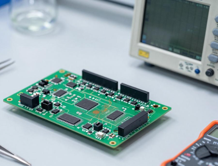
An oscilloscope or suitable data-acquisition equipment can be used to compare measured noise with the expected system noise floor.
Engineers can also introduce representative electromagnetic interference to evaluate whether the transmitter experiences:
- Measurement jumps
- ADC instability
- Communication errors
- Unexpected resets
- Analog-output fluctuations
- Common-mode interference
This type of test helps identify weaknesses in PCB layout and grounding that may remain invisible under quiet laboratory conditions.
Particular attention should be paid to analog and digital partitioning, return-current paths, sensitive sensor traces, high-speed communication interfaces, switching power supplies, and connector entry points.
Preliminary Temperature-Cycling Evaluation
A preliminary temperature test can help identify temperature-sensitive PCB or assembly problems before NPI.
The actual temperature range, dwell time, ramp rate, and number of cycles should be determined according to the product specification and applicable reliability standard. For an industrial transmitter, the validation plan may include temperatures representative of the intended operating environment rather than relying on one universal temperature range.
During testing, continuously monitor measurement accuracy and communication status.
Potential problems include:
- Measurement drift
- Intermittent communication
- Solder-joint fatigue
- Via-related intermittent opens
- Lamination defects
- Material dimensional instability
- Temperature-dependent leakage
The objective is not simply to expose the board to extreme temperatures but to correlate electrical behavior with environmental stress.
Insulation and Dielectric Withstand Testing
For isolated power, analog, communication, or sensor interfaces, perform insulation-resistance and dielectric-withstand testing according to the applicable product requirements.
The PCB review should include:
- Creepage distance
- Clearance
- Isolation slots
- Copper spacing
- Residual copper around isolation areas
- Solder-mask openings
- Contamination risks
Residual copper or insufficient spacing around an isolation barrier can create a significant safety risk.
Detecting such defects during prototype development is much less costly than discovering them after mass production.
Verify PCB Materials and Process Specifications
The prototype stage should also verify that the actual PCB materials and manufacturing processes match the approved engineering documents.
Important parameters may include:
- Laminate type
- Tg and other thermal properties
- Copper thickness
- Finished board thickness
- Surface finish
- Stackup
- Controlled-impedance requirements
- Via structure
For products exposed to thermal cycling or long service life, material substitution without engineering approval should be strictly controlled.
2. NPI Pilot Production: Validate Manufacturing Consistency
Prototype fabrication and mass production are not necessarily equivalent.
During NPI, production equipment, panelization, tooling, process windows, inspection methods, and material lots can differ from those used for prototypes. Therefore, the NPI stage should verify whether the design can be manufactured consistently at production scale.
Bare PCB Inspection
A pilot lot should be inspected before assembly.
Typical inspection items include:
- AOI inspection
- Open and short detection
- Finished board thickness
- Copper thickness
- Surface finish
- Dimensional accuracy
- Solder-mask quality
- Controlled impedance where applicable
For impedance-controlled designs, actual impedance measurements should be compared with the approved stackup and design targets.
Cross-Section Analysis
Cross-sectional analysis provides information that visual inspection cannot provide.
Depending on the product risk level, samples can be analyzed for:
- Plated-hole copper thickness
- Via-wall integrity
- Interlayer bonding
- Lamination quality
- Voids
- Delamination
- Registration
- Copper distribution
For industrial transmitters exposed to vibration and thermal cycling, reliable plated-through holes and vias are especially important because repeated mechanical and thermal stress can eventually produce intermittent electrical connections.
Assembly and Environmental Validation
After pilot assembly, environmental validation should be performed on representative finished units.
Potential tests include:
- Temperature cycling
- Damp-heat or humidity testing
- Vibration testing
- EMC testing
- Functional verification after environmental exposure
The exact conditions should follow the transmitter’s intended application and applicable standards.
During environmental testing, continuously record critical outputs instead of checking the product only before and after the test.
This approach makes it easier to correlate environmental stress with gradual measurement drift or intermittent communication failures.
3. EMC Validation: Evaluate the PCB as Part of the System
Industrial transmitters frequently operate near motors, variable-frequency drives, relays, switching power supplies, and other electromagnetic noise sources.
Therefore, EMC testing should be integrated into product validation rather than treated as a final certification activity.
Depending on the product and applicable standards, testing may include:
- ESD
- EFT/burst
- Surge
- Conducted immunity
- Radiated immunity
- Conducted emissions
- Radiated emissions
If the transmitter fails an EMC test, the investigation should include the PCB layout, grounding strategy, return path, power distribution, connector interfaces, cable coupling, shielding, and protection-device placement.
Adding more protection components is not always the most effective solution. If the PCB allows excessive noise coupling or creates an uncontrolled return-current path, the fundamental layout should be reviewed first.
4. Conformal Coating Compatibility
For industrial transmitters deployed in humid, dusty, corrosive, or outdoor environments, conformal coating may be considered as part of the environmental protection strategy.
However, coating does not automatically improve every PCB design.
Before production release, evaluate:
- Coating material compatibility
- Required coating coverage
- Keep-out areas
- Connector interfaces
- Test points
- Switches and moving components
- Heat-generating components
- Sensor interfaces
- PCB exposed-copper regions
After coating, electrical and functional tests should be repeated to verify that the coating has not introduced leakage, parasitic capacitance, insulation problems, or measurement drift.
The PCB design should therefore be reviewed together with the selected coating process.
5. Mass Production: Strengthen PCB Incoming Quality Control
Once the transmitter enters volume production, the manufacturer should establish a documented PCB quality control procedure for incoming boards.
Incoming inspection may include:
- Visual inspection
- Board thickness sampling
- Copper-thickness verification
- Surface-finish inspection
- Dimensional inspection
- Electrical testing
- Insulation testing where required
- Cross-section analysis for selected high-risk lots
Supplier certificates and inspection reports are useful, but they should not replace a risk-based incoming inspection system.
Control Critical PCB Parameters
For products with known reliability risks, maintain a controlled parameter database covering:
- Laminate model
- Tg and relevant material properties
- Copper thickness
- Stackup
- Surface finish
- Via structure
- Board thickness
- Impedance requirements
- Special manufacturing processes
Any material or process substitution should require engineering approval.
This is particularly important when a high-Tg or application-specific laminate is part of the original reliability design.
Establish PCB Traceability
Each production lot should have an identifiable traceability record.
Depending on the manufacturing system, records may include:
- PCB supplier
- Manufacturing date
- Lot number
- Material batch
- Surface-finish batch
- Inspection results
- Production panel information
When a field failure occurs, traceability allows engineers to determine whether affected units are concentrated in a specific PCB production lot.
This greatly improves the efficiency of failure analysis and corrective action.
6. Field Failure Analysis: Build a Closed-Loop Process
Field failures should not automatically be attributed to components.
The PCB itself can be a source of intermittent or latent failures, including:
- Via fatigue or intermittent opens
- CAF-related leakage or shorts
- Copper corrosion
- Insulation degradation
- Ground-via connection problems
- Solder-joint fatigue
- Delamination
- Surface-finish degradation
A structured failure analysis process can be divided into several stages.
Step 1: Reproduce the Failure
Record the original failure condition before replacing components or modifying the PCB.
Important information includes:
- Operating temperature
- Supply voltage
- Communication status
- Measurement output
- Installation environment
- Failure frequency
- Whether the failure is intermittent
Step 2: Perform Visual and Microscopic Inspection
Inspect the PCB for:
- Corrosion
- Discoloration
- Cracks
- Burn marks
- Contamination
- Solder-joint abnormalities
- Delamination
- Mechanical damage
Microscopic inspection can reveal defects that are invisible during normal visual inspection.
Step 3: Perform Electrical Analysis
Measure relevant electrical characteristics, such as:
- Insulation resistance
- Continuity
- Leakage current
- Ground resistance
- Communication integrity
- Critical signal behavior
Compare the failed unit with a known-good unit whenever possible.
Step 4: Use Cross-Section or Advanced Analysis When Necessary
If the failure cannot be identified externally, cross-sectional analysis may be required.
Depending on the suspected failure mode, engineers may use microscopy, SEM/EDS, metallographic analysis, or other appropriate analytical methods.
The goal is to determine whether the root cause originated from:
PCB design → PCB material → PCB manufacturing → assembly → system integration → field environment
rather than simply replacing failed components.
7. Long-Term Storage and Moisture Control
Storage conditions can also influence PCB reliability.
PCB bare boards should be stored according to the manufacturer’s packaging and storage requirements. Moisture-barrier packaging, desiccants, humidity indicators, controlled warehouse conditions, and FIFO management can help reduce moisture-related risks.
Although ENIG generally provides good oxidation resistance compared with some other surface finishes, it does not eliminate all environmental risks.
Moisture absorbed by PCB materials can contribute to:
- Delamination
- Blistering
- Soldering defects
- Insulation degradation
- Dimensional changes
If a PCB has exceeded its specified storage or floor-life conditions, the appropriate preconditioning or baking procedure should be determined according to the laminate, surface finish, packaging condition, and applicable manufacturing requirements.
A universal baking temperature or duration should not be applied to every PCB.
8. Complete PCB Validation Flow From Prototype to Mass Production
A reliable industrial transmitter requires a continuous validation loop rather than isolated tests.
A practical workflow is:
Prototype → PCB Electrical Validation → Environmental Screening → NPI → Bare PCB Inspection → Assembly Validation → EMC Testing → Reliability Testing → Mass Production → Incoming Quality Control → Field Failure Analysis → Design and Process Improvement
Each stage has a different objective.
| Stage | Primary Objective |
|---|---|
| Prototype | Identify fundamental electrical and PCB design risks |
| NPI | Verify manufacturing consistency |
| Pilot assembly | Validate PCB and assembly interaction |
| EMC testing | Evaluate immunity and emissions performance |
| Reliability testing | Identify latent environmental failure mechanisms |
| Mass production | Control process variation and incoming quality |
| Field analysis | Identify actual failure mechanisms |
| Corrective action | Feed lessons back into design and manufacturing |
The most important principle is to connect test results with engineering decisions. If a failure is discovered, the corrective action should be reflected in the PCB design rules, manufacturing specifications, inspection plans, and supplier-control procedures.
9. Kingda’s PCB Manufacturing Support
For industrial transmitter projects, PCB manufacturing should be treated as an integrated part of product reliability rather than simply a fabrication step.
Kingda can support industrial transmitter PCB projects through engineering review, material and stackup verification, DFM evaluation, prototype fabrication, NPI support, production inspection, impedance control, reliability verification, and mass-production quality management.
By connecting PCB design, manufacturing-process control, environmental validation, PCB quality control, and failure analysis, engineers can identify potential risks earlier and establish a more reliable transition from prototype to stable mass production.