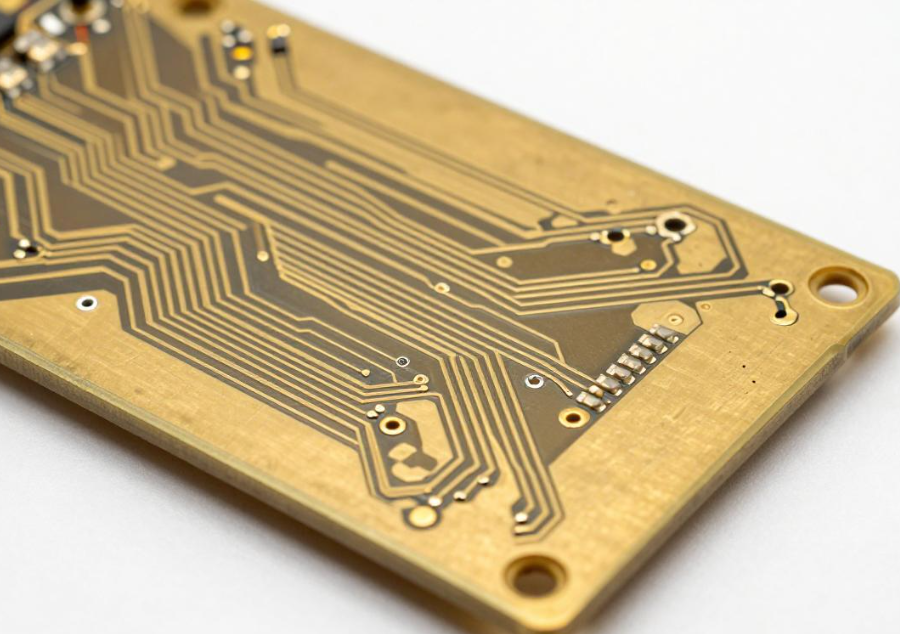
ENIG PCB technology is widely used in industrial control, automotive electronics, telecommunications, networking, and other applications that require flat contact surfaces, good solderability, and compatibility with fine-pitch packages such as BGA. However, achieving a qualified gold thickness on a prototype does not necessarily mean that the same ENIG process control can remain stable during mass production.
A common production problem occurs when XRF measurements on prototype boards meet the specification, but gold thickness becomes inconsistent across different pads on the same PCB or between boards from the same production lot. This type of gold thickness variation is more than a plating-process issue. It can affect solderability, surface reliability, contact performance, and, in some designs, high-frequency electrical performance.
For this reason, PCB manufacturing teams should evaluate not only average gold thickness but also its distribution, process capability, and stability throughout the entire production cycle. A systematic approach to gold thickness uniformity, process monitoring, and inspection can help identify risks before they develop into field failures.
1. ENIG Structure and Gold Thickness Requirements
A typical ENIG structure consists of a copper substrate, an electroless nickel-phosphorus layer, and an immersion gold layer. The gold layer is deposited through a displacement reaction between the exposed nickel surface and gold ions in the process solution.
Unlike electrolytic gold plating, immersion gold is primarily a chemical displacement process. As the exposed nickel surface becomes covered by gold, the reaction naturally slows. Therefore, the final coating thickness depends on the nickel surface condition, bath chemistry, temperature, immersion time, mass transfer, and other process variables.
IPC specifications such as IPC-4552 provide requirements and guidance for ENIG surface finishes, but the exact nickel and gold thickness requirements should be defined according to the applicable revision of the standard, product class, customer specification, and application.
For engineering control, the following parameters should be considered together:
- Minimum and maximum gold thickness
- Nickel thickness and phosphorus content
- Within-board gold thickness uniformity
- Board-to-board variation
- Lot-to-lot variation
- XRF measurement repeatability
- Solderability requirements
- Applicable reliability requirements
It is therefore insufficient to specify only a nominal gold thickness. A production specification should also define how uniformity is measured, where measurement points are located, how many samples are required, and what statistical criteria are used.
For high-reliability applications, internal control limits may be tighter than the minimum requirements of a general surface-finish specification. These limits should be established through process capability studies and customer requirements rather than treated as universal industry thresholds.
2. Typical Failure Risks Caused by Uneven Gold Thickness
2.1 Localized Surface Degradation and Contact Resistance Variation
When the gold layer is locally thin or discontinuous, the underlying nickel surface may have less protection against environmental exposure. Moisture, contaminants, and corrosive species can penetrate defects or discontinuities in the finish and gradually affect the underlying surface.
This can be particularly important for connector contacts, test pads, and other exposed contact surfaces. Inadequate surface protection may contribute to contact resistance changes or intermittent electrical behavior after storage or environmental exposure.
The risk can be difficult to detect during final inspection because a newly manufactured board may initially pass electrical and visual inspection. The problem may become more apparent after humidity exposure, thermal aging, or extended storage.
Therefore, PCB reliability evaluation should consider not only the initial appearance of the ENIG surface but also its behavior under the environmental conditions expected during the product lifecycle.
2.2 Solderability Variation and BGA Joint Reliability
Gold thickness itself is not a simple predictor of solder-joint voiding or mechanical strength. Solderability depends on multiple factors, including nickel surface condition, gold coverage, contamination, flux chemistry, solder paste, reflow profile, pad geometry, and package structure.
Excessive variation in the ENIG finish can nevertheless increase process uncertainty. A locally degraded surface may show poorer solder wetting, while other defects in the nickel/gold interface can affect solder-joint reliability.
For BGA assemblies, engineers should evaluate:
- Solder wetting and spread
- Non-wetting or de-wetting
- Voiding behavior
- Intermetallic formation
- Solder-joint geometry
- Thermal-cycle performance
- Cross-sectional structure
- Pad/interface failure modes
Rather than assuming that a specific gold-thickness variation will automatically produce a particular voiding rate, the relationship should be verified through assembly trials and reliability testing.
2.3 Black Pad Risk
Black pad is a well-known reliability concern associated with certain ENIG process conditions. It generally involves excessive or abnormal nickel corrosion during immersion gold processing and can produce a compromised nickel surface that is difficult to identify through visual inspection alone.
Uneven gold deposition may indicate unstable process conditions, but black pad should not be attributed to thin gold alone. Nickel surface condition, phosphorus distribution, bath chemistry, immersion-gold activity, corrosion behavior, and pretreatment are all relevant factors.
For this reason, ENIG failure analysis should examine the complete nickel/gold interface rather than focusing only on the measured gold thickness.
Useful analysis methods may include:
- Cross-sectional microscopy
- SEM analysis
- EDS analysis where appropriate
- Nickel and gold thickness measurement
- Surface morphology evaluation
- Bath chemistry review
- Process-history analysis
- Solder-joint cross-section analysis
2.4 Potential Variation in High-Frequency Electrical Performance
For high-frequency applications, the surface finish is only one part of the overall conductor-loss system. ENIG PCB structures can introduce electrical effects through the conductivity and thickness of the surface layers, but the magnitude depends strongly on operating frequency, conductor geometry, copper roughness, trace length, dielectric properties, and transmission-line structure.
At high frequencies, current distribution is affected by skin and proximity effects. Because gold, nickel, and copper have different electrical properties, the surface-finish structure can contribute to conductor loss.
However, it is not technically accurate to assume that ordinary ENIG thickness variation alone will always create a significant insertion-loss difference. For demanding RF and high-speed designs, engineers should evaluate the complete transmission path using simulation, material data, and measurement where necessary.
3. Root Causes of Mass-Production Gold Thickness Variation
3.1 Mass-Transfer and Edge Effects During Immersion Gold Processing
Immersion gold is a chemical reaction, so the availability and movement of reactive species at the nickel surface influence deposition behavior.
Different areas of a PCB can experience different solution exchange conditions. Board edges, isolated large pads, dense pad fields, and central regions may have different local mass-transfer characteristics.
This can contribute to spatial differences in deposition rate.
The effect becomes more important when panel design, loading configuration, bath circulation, agitation, and exposed copper distribution create significant differences in local process conditions.
A prototype run with only a small number of panels may not reveal the same variation that appears during continuous production. Therefore, ENIG process control should be evaluated under production-representative loading conditions rather than relying solely on prototype results.
3.2 Nickel Surface Condition Affects Gold Deposition
Gold thickness cannot be controlled independently of the electroless nickel layer.
The nickel surface condition can be affected by:
- Copper surface preparation
- Cleaning and degreasing
- Micro-etching
- Activation
- Nickel deposition conditions
- Nickel phosphorus content
- Nickel grain structure
- Surface contamination
- Post-nickel treatment and transfer conditions
If different regions have different nickel surface activity, the subsequent immersion-gold reaction may also vary.
This is why ENIG process control should cover the complete copper-to-nickel-to-gold process chain rather than treating the immersion-gold tank as an isolated operation.
3.3 Dynamic Bath Chemistry Changes During Mass Production
During continuous production, the process solution changes over time.
Gold species are consumed, reaction by-products accumulate, and the concentration of certain chemical components may change. Temperature, pH, contamination, filtration efficiency, agitation, and chemical replenishment can also influence deposition behavior.
If production relies only on first-piece approval, the process may gradually drift after the initial inspection.
A more robust control system should include:
- Defined bath-control parameters
- Scheduled chemical analysis
- Replenishment based on measured conditions
- Equipment and circulation checks
- In-process XRF monitoring
- Lot traceability
- Trend analysis and corrective-action procedures
This approach allows engineers to identify gradual drift before it develops into large-scale gold thickness variation.
3.4 PCB Layout and Panel Structure Affect Plating Uniformity
The physical structure of the PCB can also influence chemical exchange.
Copper distribution, pad density, exposed nickel area, panelization, tooling, clamps, process rails, and board spacing may all affect solution flow and local mass transfer.
Examples include:
- Large exposed copper regions adjacent to dense fine-pitch pads
- Highly concentrated BGA areas
- Large isolated pads
- Uneven copper distribution
- Tooling that partially shields active surfaces
- Inappropriate panel spacing
- Mixed products with significantly different exposed areas
Consequently, PCB DFM should consider surface-finish requirements during the design stage rather than treating ENIG as a purely manufacturing-side issue.
4. Engineering Risk Checklist Before Mass Production
Before releasing an ENIG PCB design to volume production, engineers should review the following items.
4.1 Define More Than Nominal Gold Thickness
The manufacturing specification should clearly define:
- Required gold thickness range
- Nickel thickness
- Measurement method
- XRF calibration requirements
- Measurement locations
- Sampling quantity
- Within-board uniformity criteria
- Lot-to-lot variation criteria
- Acceptance and rejection rules
If statistical limits such as CV or maximum-minimum deviation are used, they should be established according to the product requirement and validated manufacturing capability.
4.2 Separate Prototype Validation From Mass-Production Validation
Prototype approval demonstrates that a process can produce acceptable boards under a specific condition. It does not automatically prove long-term process capability.
Before mass production, consider a production-representative validation run covering:
- Actual panelization
- Representative copper distribution
- Normal production loading
- Relevant board dimensions
- Expected surface area
- Actual bath-control conditions
- Multiple measurement locations
- Multiple boards across the production sequence
This can reveal process drift that is invisible during a small prototype build.
4.3 Prioritize Critical Locations
Not every pad has the same functional importance.
Measurement locations should be selected based on:
- BGA and fine-pitch packages
- Connector contacts
- High-speed transmission-line interfaces
- Critical test points
- Large isolated pads
- Board-edge areas
- Center areas
- Areas with unusual copper density
A balanced sampling plan provides more useful information than simply measuring convenient locations.
4.4 Use XRF as a Process-Control Tool
Visual inspection cannot reliably determine actual gold thickness.
XRF inspection provides a practical non-destructive method for measuring coating thickness and can be used at incoming, in-process, and final inspection stages.
For production control, engineers should also consider:
- XRF calibration and verification
- Measurement repeatability
- Fixed measurement locations
- Multi-point sampling
- Statistical trending
- Outlier investigation
- Correlation with cross-sectional analysis when necessary
The objective is not simply to prove that one board is qualified, but to demonstrate that the process remains stable throughout production.
5. Building a Closed-Loop ENIG Process-Control System
A stable PCB manufacturing process requires more than final inspection. The most effective strategy is to connect design, pretreatment, nickel plating, immersion gold, inspection, and assembly feedback into one control loop.
A practical control framework can include:
PCB DFM → Pretreatment → Electroless Nickel → Immersion Gold → XRF Inspection → SPC Analysis → Corrective Action → Production Verification
At the design stage, engineers can reduce potential variation by reviewing panelization, copper distribution, pad geometry, exposed surface area, tooling regions, and critical electrical structures.
During production, the supplier should monitor chemical conditions, equipment performance, loading configuration, process time, and bath maintenance.
During inspection, XRF inspection data should be collected at predefined locations and analyzed for trends rather than used only for pass/fail judgment.
When abnormal variation occurs, engineers should trace the issue backward through:
Gold Bath → Nickel Surface → Pretreatment → Panelization → PCB Design
This approach is more effective than simply increasing inspection frequency after a defect has already appeared.
6. How Kingda Can Support Stable ENIG Production
For high-volume PCB manufacturing, gold thickness consistency should be managed as a complete process-capability issue rather than a single plating parameter.
Kingda can support ENIG PCB projects through engineering review, manufacturing-process control, panelization assessment, XRF measurement, production monitoring, and quality verification.
For demanding applications, the key is to establish measurable requirements before mass production and verify process stability with representative production data. By combining PCB DFM, ENIG process control, gold thickness uniformity, and XRF inspection, engineers can identify potential risks earlier and build a more consistent path from prototype approval to stable mass production.