High Quality PCB Design: Placement, Thermal and Signal Priorities
On a precision analogue board, or on a low-frequency digital board where a millivolt of noise matters, the quality of the result is decided long before the first trace is drawn. High quality PCB design at these signal levels is mostly a question of where the parts are, what is next to what, and how the return currents find their way home. The rules below apply most directly to instrumentation, sensor interfaces and audio, and they cost nothing to follow.
Placement Decides the Rest
Component placement is the single largest determinant of final performance. A placement that groups each function into a compact block with its own local supply and ground, and that puts the noisy blocks away from the quiet ones, makes the routing almost self-solving. A placement that scatters the parts makes every subsequent decision a compromise.
The practical method is to work from a block diagram rather than from the schematic. Draw the functional blocks, mark the signals that pass between them, and place the blocks in the order the signal travels. Then place the parts inside each block.
Mechanical Fit and Mechanical Stress
The board has to survive installation. Mounting holes and cut-outs have to be positioned so that no cross-section of the board becomes a weak point, and the distance from a hole to the board edge should generally exceed the hole diameter. Where a connector protrudes through an enclosure panel, it has to be fixed in a way that takes the insertion force rather than transferring it to the solder joints.
Vibration is the usual failure mechanism rather than a single overload. Heavy components, large connectors and anything mounted on a bracket should be placed near a mounting point or a stiffener rather than in the middle of an unsupported span.
Thermal Isolation in Precision Designs
thermal isolation matters more than heat removal on a precision board. A regulator or a power amplifier that runs 30 degrees above ambient will shift the offset of any precision amplifier placed next to it, and it will change the value of any component whose temperature coefficient is not zero. Put the dissipating parts at one end of the board, keep the sensitive front end at the other, and use copper and slots deliberately to steer heat away from the parts that care.
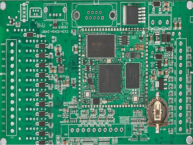
A slot under a hot device is an effective thermal barrier, and it costs nothing but a routed outline. Where a barrier is not practical, give the sensitive part a local ground pour and keep it out of the thermal shadow of the power stage.
Keeping Weak Signal Circuits Away From Strong Ones
The classic separation rules still work: weak signal circuits apart from strong signal circuits, analogue apart from digital, high frequency apart from low frequency, high impedance nodes kept short, and the highest-impedance node on the board given the most protection. In practice this means that the input of a high-impedance amplifier should be a short trace with a guard or a grounded trace beside it, and that this node should never run past a switching node or a digital bus.
Crosstalk between a sensitive trace and an adjacent one is a function of the distance, the parallel run length and the impedance of the victim node. A high-impedance node couples far more than a low-impedance one, so the same spacing that is adequate for a logic line can be insufficient for an amplifier input.
Grounding in a Mixed-Signal Design
Grounding is where most of these designs succeed or fail. The starting point is a single continuous ground plane with careful control of where each return current flows, not a set of islands labelled analogue and digital. A split ground plane forces the return path of any signal crossing the split to detour, and the resulting loop radiates and couples.
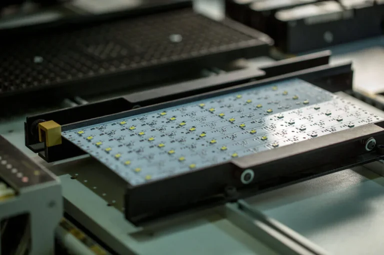
The workable compromise is to keep the converters on the boundary between the noisy and quiet areas and to give each quiet block a local pour connected to the main plane at one point. Mixed-signal PCB design guidelines describes the arrangement in more detail, and Ground routing and power trace planning covers how the plane structure is planned before routing.
Appearance and Its Limits
A tidy layout is easier to inspect, easier to modify and easier to document, so neatness has real value. It should not, however, override the electrical requirements. On a board that will be enclosed and never seen, priority belongs to the routing and the grounding, even when the result looks less regular than a grid-aligned placement would. The exception is a board that will be photographed or sold as a visible product, where the cosmetic requirement is a legitimate design input.
Decoupling and Local Supply
Every active device needs its own local charge reservoir, placed so that the loop from the capacitor to the pin and back to ground is as small as possible. On a precision board the supply rejection of the amplifier is a specification, not an assumption, and it degrades with frequency, which is exactly where the decoupling has to work.
Keep the supply routing for the analogue section separate from the digital section until they meet at the regulator or the star point. Placement order and pad positioning explains how the pad geometry and the placement order interact with these decisions.
Verification
Placement Order in Practice
Work in a fixed order and the placement will converge quickly. Start with the parts whose position is already decided by the enclosure: connectors, mounting holes, displays, switches and anything that must line up with a panel cut-out. Then place the converters, amplifiers and references that define the analogue signal chain, because their relative positions determine the length of the sensitive traces. Then place the digital section, keeping it physically distinct, and only then fill in the decoupling and the small support components.
After the blocks are in place, check the result against the mechanical drawing and against the thermal plan before routing starts. It is much cheaper to move a power stage to the far end of the board at this point than to discover after assembly that it warms the reference by ten degrees. A second pass with the block diagram beside the layout will usually reveal one or two parts that ended up in the wrong region.
A precision design should be measurable. Include test points on the supply rails, on the reference, and on the amplifier output, and measure the noise floor with the digital section active and idle. A board that meets its specification on a bench with the clock stopped has not been tested.
FAQ
Is a low-frequency board easier to lay out? Not necessarily. Below about 50 MHz the geometry is forgiving, but the analogue performance still depends on placement, grounding and thermal design, and those are the parameters that decide whether the board meets its noise specification.
Should analogue and digital grounds be separated? Usually not into two planes. A single ground plane with controlled return paths is more predictable. Splitting is occasionally justified when a converter defines the boundary, and then it should follow the data sheet rather than a habit.
How much space should be left around a sensitive node? As much as the layout allows, and at minimum enough that the spacing rules for the highest-impedance node on the board are satisfied. Guard traces and local pours are the fallback when space is not available.