Analog Digital Partitioning and Ground Strategy on Mixed Boards
Analog and digital circuits share a board happily as long as they are not allowed to share return currents. Most mixed signal problems are not caused by the analog signal itself but by the reference it is measured against, which has been polluted by switching currents from the digital side. Analog digital partitioning is the practice of controlling where those currents flow, on the board and on the die.
Where Mixed Signal Problems Come From
A digital output switching in a few nanoseconds draws current from its supply and returns it through the ground plane. That return current follows the path of least impedance, which at high frequency means the path directly under the trace. If an analog trace runs beside a digital trace, the shared return path couples the switching noise into the analog circuit, and the error appears as offset, noise or distortion depending on the circuit.
The second source is the power supply itself. A shared rail between a converter and a comparator couples the load steps of the digital device into the analog supply. Both mechanisms are layout problems rather than component problems, which is why partitioning decisions belong to the layout stage and cannot be fixed by changing an amplifier later.
Partitioning the Board into Regions
Draw the board as two regions before placing anything: an analog region containing converters, references, filters and sensors, and a digital region containing the processor, memory and interfaces. Place components within their region, then decide how the two communicate. Signals that cross the boundary should do so at a single, defined point, ideally with a series termination or a buffer that limits the current that can flow in either direction.
Keep the regions physically separate rather than interleaved. Interleaving looks efficient in board area but creates dozens of opportunities for crosstalk and return current sharing. A clean boundary costs a little area and removes most of the risk, and it makes the design review straightforward because the crossing points are visible on the drawing.
Ground Strategy for Mixed Signal Boards
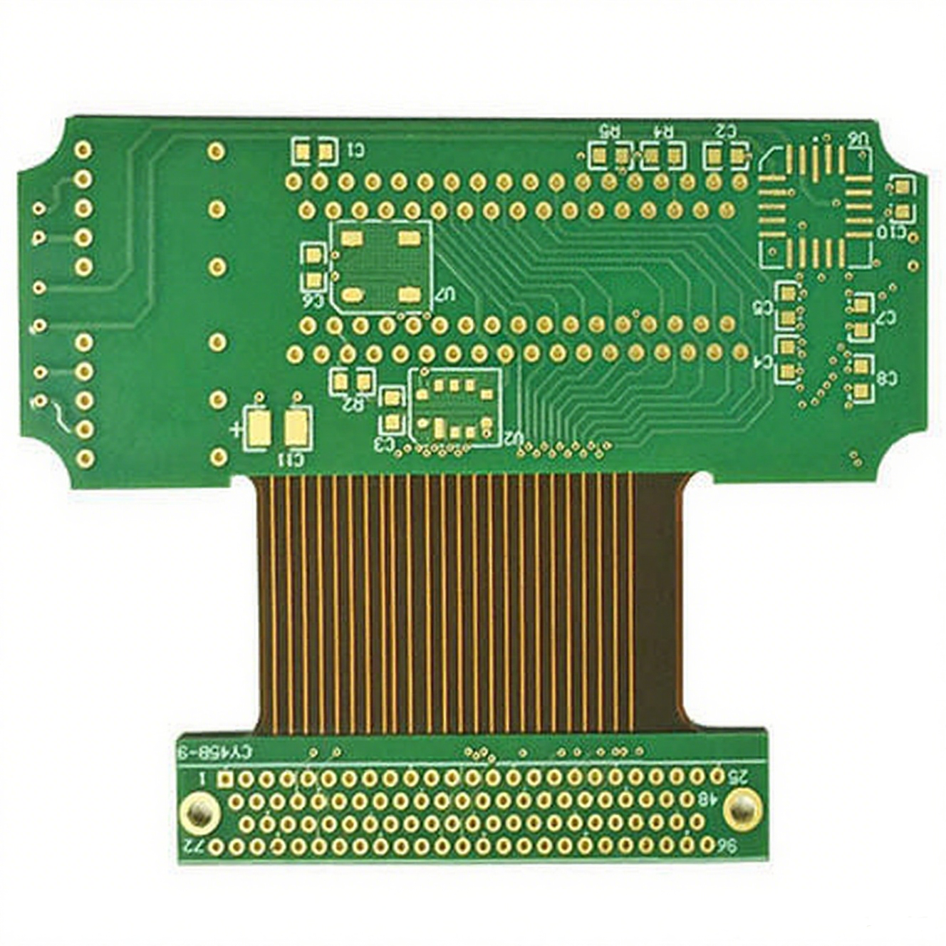
The ground strategy is the most debated part of mixed signal layout. A single continuous ground plane with the analog components placed in one area is the modern default, because a continuous plane avoids the return path discontinuities that a split plane creates. What matters is that no digital return current is forced to flow under the analog components.
Where a split is used, the analog and digital grounds meet at exactly one point, usually under the analog to digital converter, so that the converter’s own reference determines the relationship between the two. Multiple connections between split grounds create loops that carry an unpredictable share of the return current. Whichever approach is chosen, the converter datasheet’s recommended arrangement takes precedence, because the internal structure of the device determines what it expects.
Converter Placement and Reference Design
Place the converter at the boundary between the two regions, oriented so that its analog pins face the analog side and its digital pins face the digital side. This single decision simplifies everything downstream: the analog input network stays short and quiet, and the digital output bus runs into the digital region without crossing sensitive circuitry.
The voltage reference deserves its own treatment. Place the reference close to the converter, filter its supply, and keep its output trace away from digital signals. Route the reference and its ground as a pair to each device that uses it, and avoid sharing a reference trace between devices that switch at different times. A reference that moves by a fraction of a millivolt produces a visible error in a high resolution measurement.
Power Distribution and Filtering
Feed analog rails from a separate regulator or from a filtered branch, not directly from the digital rail. A ferrite bead followed by bulk and bypass capacitance forms a simple filter, but the bead must be chosen for the current and the frequency range of interest, otherwise it saturates and passes the noise it was meant to block.
Decouple each analog device locally, keep the loop small, and connect the capacitor ground to the same ground the device uses. Where an analog rail crosses to the digital region to feed an interface, filter it at the boundary rather than at the far end. Review the arrangement against mixed signal PCB design guidelines, which cover the same principles from the converter manufacturer’s point of view.
Return Current Path Control
The single most effective rule is to route every trace so that its return current has a defined, uninterrupted path directly beneath it. On a continuous plane this happens automatically when the plane is unbroken, so any slot or cut in the plane must be justified. Where a trace must cross a plane boundary, place a stitching capacitor across the split to provide a path for the return current.
Apply the same reasoning to cables that leave the board. A signal that leaves through a connector returns through the connector’s ground pins, and the current flows from the ground plane to those pins. Keep the connector ground pins and the plane tie points close together, following ground routing and power trace planning practice so that cable currents do not flow across the analog region.
Trace Routing Rules at the Boundary
Never route a digital trace through the analog region, even if the geometry makes it convenient. Where a crossing is unavoidable, run it on a layer adjacent to the ground plane rather than on the analog side’s surface layer, and keep the crossing perpendicular to analog traces rather than parallel. Perpendicular crossings minimize the coupled length.
Keep analog traces short and wide enough to control their impedance, and surround sensitive ones with ground rather than relying on spacing alone. Differential analog signals should be routed as pairs with matched length, and single ended signals should have a defined return path through the same region. Following EMI suppression design principles keeps the intent obvious to anyone reviewing the layout later, which protects the design through future revisions.
Verification and Common Mistakes
Verify the layout by measurement rather than by inspection. Inject a known signal into the digital side and observe the analog output with a spectrum analyzer or a low noise oscilloscope, then repeat with the digital load at maximum. Any change in the noise floor between the two conditions points to a coupling path that can be traced back to a specific region of the board.
The recurring mistakes are predictable: a converter placed in the middle of the digital area, a reference shared between two devices, a plane split with several connections, and a power rail shared without filtering. Each of them is easy to avoid in the design stage and expensive to correct after the enclosure is built. gopcb builds mixed signal boards regularly and can review the partitioning, the ground strategy and the filtering plan before the layout is committed.
FAQ
Should analog and digital grounds be split? Usually not on a modern board with a continuous plane, provided the analog components are grouped together and no digital return current passes beneath them. Split grounds are appropriate when the converter datasheet requires them, with a single tie point.
How far apart should the two regions be? Far enough that a digital trace cannot run parallel to an analog trace for a meaningful distance, and far enough that the analog return path stays clear. In practice, a separation of a few millimeters plus a defined boundary usually suffices.
Is a ferrite bead enough to isolate an analog rail? It helps when chosen for the actual current and frequency, and it is not a substitute for local decoupling and a clean return path. Beads that saturate with the load current behave like a resistor and lose their filtering effect.