Solder Joint Visual Inspection And Acceptance Criteria Visual inspection is the oldest and still the most common method of judging a solder joint. It is fast, it needs no capital equipment beyond a light and a lens, and it finds the defects that matter most in production. It is also…
Dielectric Loss Tangent Selection Guide The loss tangent of a laminate is the fraction of the energy in the field that is turned into heat as the signal passes. It is quoted as a small number, it changes with frequency and temperature, and it is the property that separates a…
Stencil Frame Tension and Mesh Mounting for Printing A stencil has to sit flat against the board, and it has to be flat while a squeegee presses it down and pulls across it. That flatness comes from tension in the mesh or the foil. When tension falls, the stencil sags…
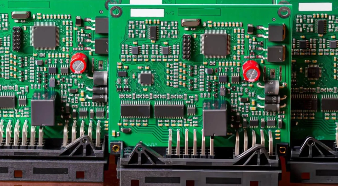
Electrolytic Capacitor Placement And Loop Area Control An electrolytic capacitor is the largest component in most power circuits and the one whose position has the widest consequences. It sets the area of the loop that the switching current flows around, it is the component that dries out first when it…
Flex Rigid: Preparation, Placement and Process Control A flex rigid board is two constructions joined into one. Part of the board is a stack of rigid laminates; part of it is a thin flexible layer that can be bent; and the region where the two meet is the transition zone.…
CTE Mismatch PCB Design Guide CTE mismatch is the difference in thermal expansion between the materials in an assembly. A laminate expands by about fifteen parts per million per degree, a ceramic body by six, and a metal package by twelve. Every temperature change therefore moves the parts by different…
Backdrilling: Design Rules and Process Limits A plated through hole that connects an inner layer to the outside is drilled through the whole board, so the part of the barrel below the layer that matters is a length of copper that carries no signal. That unused length is the via…
Panel Cleaning Before Lamination and Coating Steps Between the plating line and the lamination press, and again before solder mask is applied, the panel has to be clean. Contamination at those points does not show up immediately: it appears later as a delaminated inner layer, a lifted mask or a…
Design For Testability: Design Rules and Process Limits Design for testability is the practice of making a board easy to verify. It is a layout decision that is made once, early, and that decides whether the product can be tested in a minute or debugged for an hour. A design…
Gold Finger Chamfer And Bevel Depth Control A gold finger edge connector works by sliding. The board is pushed into a socket, and the leading edge of the board has to guide itself between the contacts without catching on them, without bending a contact spring and without removing metal from…