PCB Silkscreen Legend And Clearance Rules The silkscreen, or legend, is the printed information on a board that a human reads: the reference designators, the polarity marks, the connector pin numbers, the part outlines and the warnings. It is the cheapest layer of the board and the one most often…
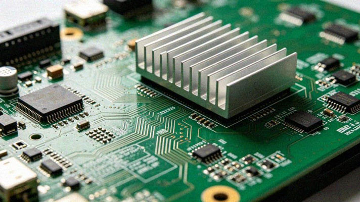
Component Clearance: Preparation, Placement and Process Control Component clearance is the space that two parts need between them, and it is always larger than the space they occupy. The extra distance is for the placement nozzle, the soldering process, the inspection camera and the rework tool. A board that is…
Length Matching and Timing Skew Control in PCB Routing Two signals that leave a driver at the same instant must arrive at the receiver within a defined window of each other, or the interface will read the wrong data. Length matching is the practice of adjusting trace lengths so that…
Differential Pair: Preparation, Placement and Process Control A differential pair carries a signal on two conductors and reads the difference between them. That arrangement rejects common mode noise, halves the effective switching current and gives a predictable impedance, but only if the two traces stay coupled and matched along the…
Conformal Coating Masking And Keepout Design Conformal coating is applied after assembly to protect the board from moisture, contamination and electrochemical migration, and the coating has to be kept away from the features that must remain accessible or that cannot tolerate it. That is the masking requirement, and it is…
BGA Escape Routing Design Guide BGA escape routing is the work that a ball grid array forces on the designer before any functional trace can be drawn. The package hides its connections underneath, so every signal has to be routed out from the inside of the array to the rest…
EMI Shielding Can Design And Via Stitching A shielding can is a metal cover soldered or clipped over a circuit to stop radio frequency energy leaving it, and sometimes to stop energy entering it. The can itself is simple; the design problem is the ground connection that makes it work,…
Back Drilling Design Guide Back drilling is the process that removes the unused part of a via barrel after plating. That unused part is the stub, and on a thick board it behaves as an open ended transmission line that resonates inside the band of a high speed link. The…
Mounting Hole Design, Plating And Clearance A mounting hole looks like the simplest feature on a printed circuit board and is one of the most frequently mis-specified. It may be a plain hole through the laminate, a plated hole that connects the board to a chassis, a hole with a…
Differential Pair Via Design Guide Every differential pair has to change layers somewhere, and the transition is where most of the signal integrity problems in a high speed link are created. A differential pair via is not two independent vias; it is a coupled structure whose symmetry decides how much…