



PCB Inspection Methods for Prototype and Production Boards No single test verifies a printed circuit board. Each inspection method sees a different class of defect, and a program that relies on only one of them will release boards with defects that the method cannot detect. Building an inspection plan means…
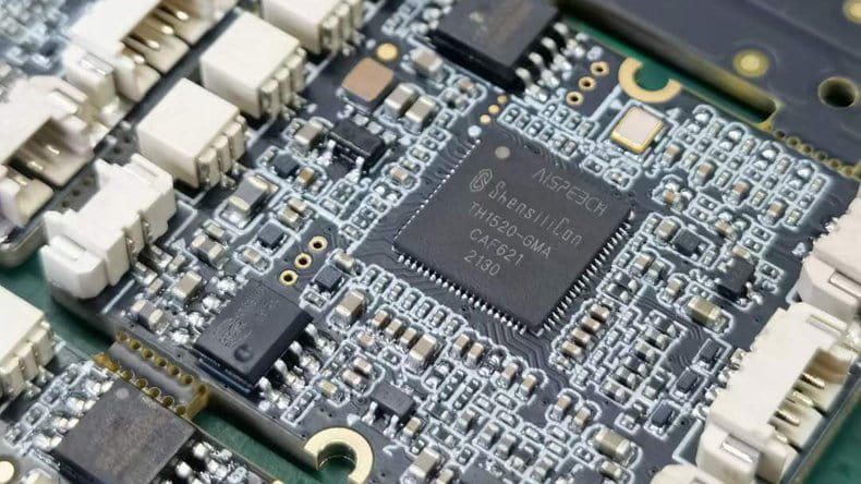
Selective Soldering Nozzle and Process Control Selective soldering exists because a board can be too complex for a wave and too populated for a hand iron. A nozzle delivers a small wave to one joint at a time, which gives the process the control of hand soldering and the repeatability…
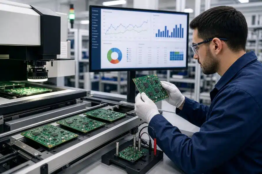
Deburring And Brushing Of PCB Panels Cuts and holes in a printed circuit board leave material that should not be there. Drilling pushes a small lip of copper out of every hole on the exit side, routing leaves a burr along the outline, and the edges of both carry resin…
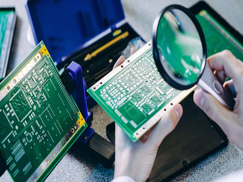
Edge Plating Requirements for PCB Fabrication Edge plating is copper that wraps from the top side of a board around the cut edge to the bottom side. It is used for shielding continuity, for high current paths between layers, for soldering a board into a metal frame and for the…
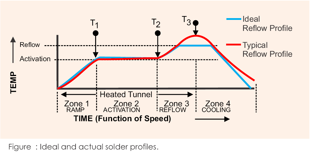
Board Edge Plating And Routing Quality Control The edge of a printed circuit board is the last surface to be produced and the first to be handled. It is cut from a panel that contains several boards, and the way it is cut decides whether the laminate delaminates, whether the…
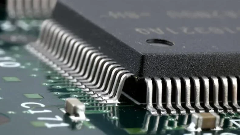
Printed Circuit Board Advantages over Alternative Wiring Hand wired circuits still exist in laboratories, but every product that must be manufactured more than once ends up on a printed circuit board. The reasons go beyond convenience: a board gives repeatable geometry, controlled electrical characteristics, mechanical support and a surface that…
Surface Energy and Wettability Control in PCB Assembly Every soldering, coating and bonding process depends on a liquid wanting to spread over a solid. That tendency is described by the surface energy of the solid and the surface tension of the liquid, and it is easily destroyed by a fingerprint,…
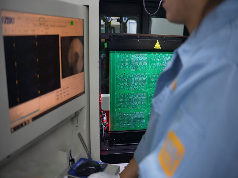
Board Depaneling Selection for Production Assembly Separating finished boards from their panel looks like the simplest step in the process and is responsible for a surprising share of field failures. Board depaneling introduces mechanical stress, and the way that stress is applied decides whether a ceramic capacitor cracks, a solder…
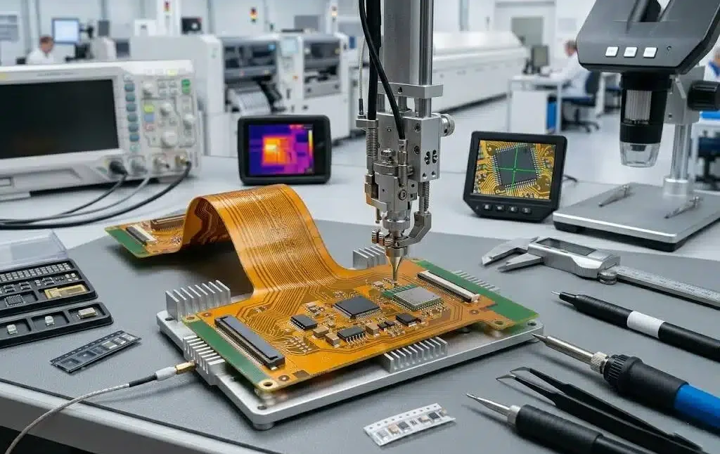
PCB Strain Relief Design Guide PCB strain relief starts from a simple observation: most board failures that arrive as electrical faults began as mechanical ones. A cable is pulled, a connector is levered, a flex tail is bent once too often, and the load ends up at a solder joint…
Stencil Nano Coating and Its Effect on Paste Release A stencil aperture is a small well with vertical walls, and solder paste has to leave it completely when the board separates. As apertures shrink, the paste increasingly prefers to stay where it is, clinging to the walls and to the…
