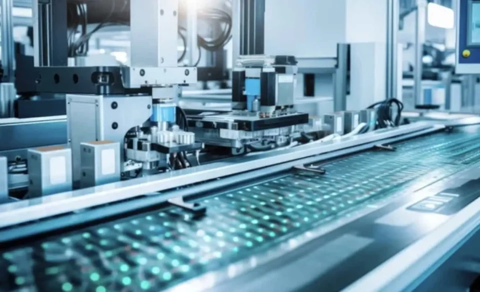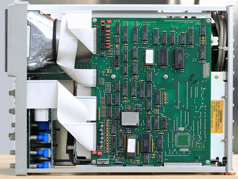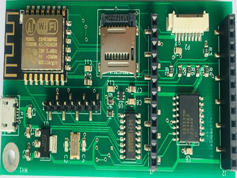
Automated PCB Assembly: How a Full Line Works A fully automated pcb assembly line turns a set of design files and a bill of materials into tested boards with very little human intervention between the two. The steps are well established, but the way they interact decides yield, and understanding…
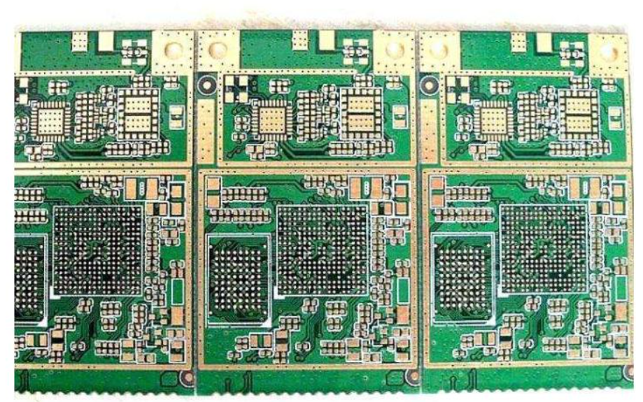
Solder Mask and Legend: Functional Not Cosmetic The mask and the legend are applied at the end of fabrication and they are the layers most often revised for cosmetic reasons, which is why they are also the layers where a change can quietly invalidate a qualification. Treating them as functional…
SMT Land Pattern Design and Density Levels Explained The land pattern is the interface between a component and the board, and it is usually copied from a library without a second look. That is a mistake, because the same package can be laid out with different density levels, and the…
PCB Lead Time: What Really Drives the Schedule Lead time is the question every purchase engineer asks and the answer that is hardest to give precisely, because it depends on the board, the quantity and the factory rather than on a single figure. Understanding what actually consumes the days makes…
Ethernet Magnetics: Design Rules and Process Limits An Ethernet port looks simple from the outside, but between the RJ45 jack and the PHY there is a small block of transformers, chokes and resistors that decides whether the link is reliable. The ethernet magnetics provide isolation between the cable and the…
Counterfeit Component Detection in Incoming Inspection Counterfeit components are not only a problem of hostile suppliers. Parts rejected at one factory, pulled from scrapped assemblies, or relabelled to a higher grade all find their way into distribution, and they arrive looking entirely normal. Incoming inspection is the last point at…
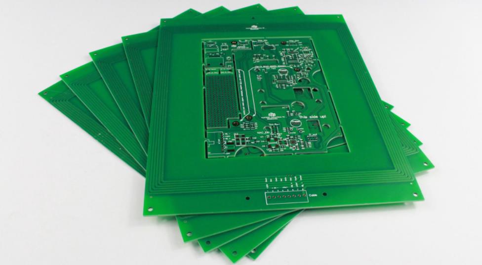
Gerber Files and Prototype Data: What to Send a Fabricator Most delays on a prototype order are not caused by the fabrication itself. They are caused by a file package that needs clarification, and every question from the fabricator costs a day. Sending a complete, self-consistent set of Gerber files…
Copper Pours: Stitching, Islands and Thermal Relief Copper pours are used on almost every board and understood on almost none. A pour that is connected at one point behaves as an antenna, one that is connected everywhere behaves as a plane, and the difference between the two is decided by…
Utilisation: Reading a PCB Quotation: Where the Cost Comes From An invoice for a printed circuit board is a statement of a process, and a designer who can read it can tell where the cost has been incurred and what to change. The breakdown is not usually itemised, and the…
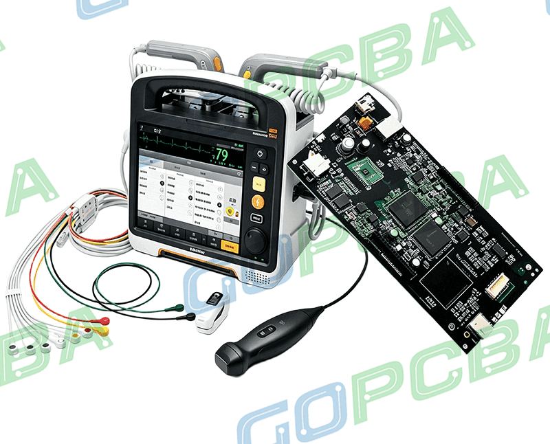
Wearable PCB Design for Medical Devices: Flex and Power A wearable medical device has to be small, comfortable, electrically safe against the skin and able to run for days on a battery the size of a fingernail. Those requirements pull in different directions, and the board is where the compromise…