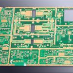
Copper Pours: Stitching, Islands and Thermal Relief
Copper pours are used on almost every board and understood on almost none. A pour that is connected at one point behaves as an antenna, one that is connected everywhere behaves as a plane, and the difference between the two is decided by how the stitching is placed.
Why a Pour Is Added
A pour is added for several reasons: to carry heat away from a device, to provide a return path, to balance the copper distribution for lamination, and to reduce the amount of etchant consumed. Each of those has a different requirement.
The requirement determines the design. A thermal pour needs a large area connected to the device; a return pour needs stitching to the reference plane; a balance pour needs only to be unconnected and evenly distributed. Our copper balance notes describe the third.
Islands and Their Disconnection
A pour that is broken into islands by the routing leaves pieces of copper connected to nothing. An unconnected island is harmless electrically and harmful in every other respect, because it can move during lamination and it can act as a small resonator.
The layout tool usually provides a check that identifies unconnected islands, and the check should be run rather than the islands removed by eye. Where an island is large, it can be connected to the plane with a via instead of being deleted.
<img src="https://www.gopcba.com/wp-content/uploads/2026/08/5lRxYcI_XX3h4-BipULu61gw3L-RLFsml7hKUIgIa_VH27O-NxAY4kwXW-anx9eybam9Oi6IQU1Z6Ikty88PAv96DDaMknpa0qy0QqunYNmrcMEdlDPmwA9BhROsA1D9O822fX5pNp5xOnz-tn-6Lh4qo_E3y_iCy67kzO0tfMdAZvnqq2fkM1twbpuC3hx.jpg" alt="Copper pour on a PCB with stitching vias” />
Stitching and Its Spacing
The vias that connect a pour to the plane should be placed at intervals short compared with the wavelength of the highest frequency of interest. A rule of thumb is a fraction of a wavelength, and the fraction is chosen so that the pour behaves as a plane across the band.
The stitching also performs a second function: it keeps the potential of the pour uniform, so that the return current does not have to travel to a distant connection point. Our mixed signal notes describe the principle.
Hatched or Solid
A solid pour is better electrically and worse mechanically on a flexible or thin board, where the copper makes the material stiff and prone to delamination. A hatched pour reduces that effect at the cost of a slightly higher impedance.
The hatch pattern introduces its own constraint: the openings have to be wide enough for the process to clear the resist and the etchant, which is a limit of a few tenths of a millimetre.
Pour and Thermal Relief
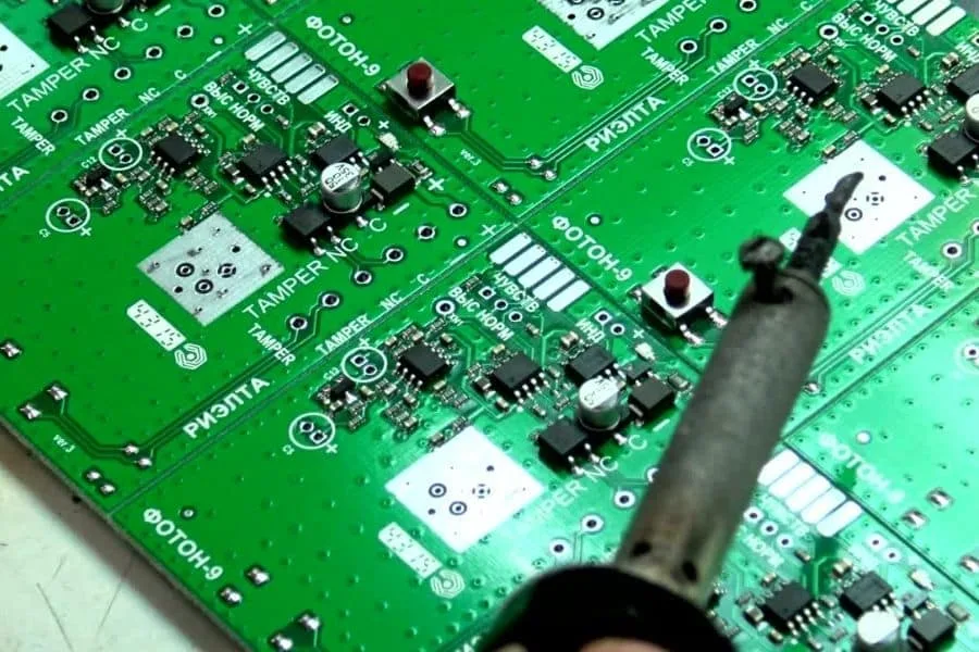
A pad connected directly to a pour conducts heat away during soldering, which is a problem for hand assembly and for wave soldering. Thermal relief spokes reduce the conduction while keeping the electrical connection.
The trade is a small increase in the impedance and a small reduction in the current capacity, which is acceptable for a signal pad and not for a power pad. The two cases should be treated separately rather than with a global rule.
Pour and the Board Edge
A pour that reaches the board edge will be cut by the routing tool, which leaves a burr and can lift the mask. The clearance between the pour and the outline should be at least a couple of tenths of a millimetre.
The same applies to cut-outs and to the panel border, where the pour should stop short of the routing path. Our board outline notes describe the tolerances.
Pour and Impedance
A pour close to a trace changes the impedance of that trace, because it acts as a partial reference. The effect is small when the pour is far and significant when it is close, and it is one of the reasons a controlled impedance trace should be designed with a defined reference rather than whatever copper happens to be nearby.
Where a controlled line runs beside a pour, the spacing should be included in the calculation. Our impedance notes describe the geometry.
Documenting the Intent
The drawing or the notes should state which pours are to be stitched, which are to be left isolated and what the clearance to the outline is. A pour with no stated purpose will be modified by whoever touches the layout next.
Recording the intent also allows the pour to be checked against the requirement. A thermal pour that has been stitched to the plane in a way that fragments it no longer performs the function it was added for.
Additional Considerations for This Build
Practical attention to hatched pattern pays for itself here, because it decides whether the finished board behaves as the drawing intended. Where the requirement is not stated on the fabrication drawing or in the assembly notes, the shop has to assume a default, and that default is rarely the value the design was simulated with. Stating hatched pattern explicitly, together with the tolerance that applies, removes the assumption and keeps the result predictable from batch to batch.
Process Control and Verification
On a design of this kind, stitching is the item that decides how the rest of the board is arranged. The process window is set by the narrowest step in the flow, so an improvement anywhere else shows up as margin rather than as yield until that step is addressed. A short note on the drawing about handling, storage or packaging is often worth more than an extra decimal place on a tolerance.
Where a value sits close to a process limit, the drawing should say so, since the shop can then open the process window rather than working to a nominal figure that carries no tolerance. A stack-up that is drawn rather than described removes most of the ambiguity from a quotation, and it lets the fabricator price the board against the dielectric and copper weights that will actually be used.
Where the requirement is not written down, the shop supplies its own default, and the default is chosen for the process rather than for the design.
Process Control and Verification
On a design of this kind, stitching is the item that decides how the rest of the board is arranged. The process window is set by the narrowest step in the flow, so an improvement anywhere else shows up as margin rather than as yield until that step is addressed. A short note on the drawing about handling, storage or packaging is often worth more than an extra decimal place on a tolerance.
FAQ
Should a pour always be stitched? It should be stitched when it acts as a return path or as a plane. Where it exists only for balance, stitching is unnecessary and may even be undesirable if the pour is meant to be isolated.
Can a pour be used instead of a plane? On a two-layer board, a stitched pour on the far side of the routing gives most of the benefit of a plane. The limit is reached when the routing fragments the pour into pieces that are too small to behave as a return path.
What does gopcb check about pours? We check the clearance to the outline and to the routed features, the hatch pattern where one is used, the balance of copper between layers and the presence of islands that are connected to nothing. Where a pour is fragmented we report it rather than removing it silently.