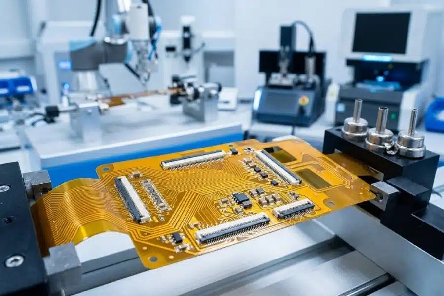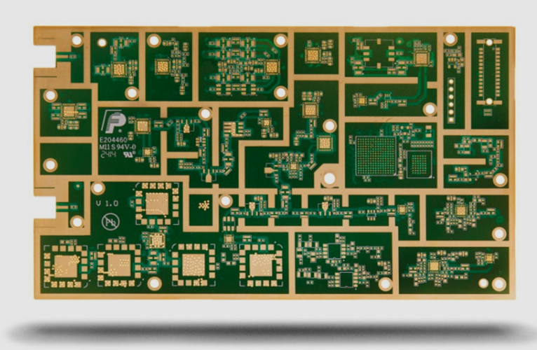
PCB Laser Drilling: UV, CO2, and Hybrid Systems Compared Microvias are what make high-density interconnect possible, and almost all of them are formed by PCB laser drilling rather than by a mechanical bit. A laser removes dielectric without applying mechanical force, which allows holes far too small for a drill…
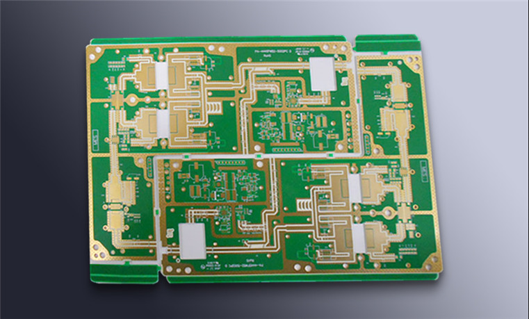
Laser Drilling Defects in PCB Microvia Fabrication As conductor widths fall and pad pitches shrink, the mechanical drill reaches a limit. A bit that is small enough to produce a 0.15 mm hole is fragile, slow, and difficult to control to the depth required for a blind via. Laser drilling…
Clearance Rules: Electrical and Non-Electrical Spacing Every pair of copper features on a board has a spacing between them, and that spacing is either dictated by electricity or by manufacturing. Designers who treat all clearances as one category tend to over-constrain the layout in some places and under-constrain it in…
Conformal Coating and Surface Insulation Resistance The purpose of a coating is usually described in terms of water and dust, and those are real threats. The mechanism that actually destroys assemblies, however, is more specific: a thin film of moisture on the surface of the board, combined with contamination, forms…
PCB Layout Design: Grid, Placement and Spacing Rules Routing gets the attention, but most of a board’s electrical and manufacturing problems are decided before the first trace is drawn. A PCB layout design that begins with placement and finishes with routing costs less to complete, is easier to inspect, and…
PCB Design and Production: Schematic to Volume Manufacturing Every electronic product passes through the same sequence: a specification becomes a schematic, the schematic becomes a physical board, a prototype proves the concept, and a factory reproduces it thousands of times. What makes that sequence interesting is that PCB design and…
PCBA Assembly Methods for Single-Sided and Double-Sided Boards The assembly route for a board is decided long before the first unit is built, and it is usually fixed by the mix of components the design contains. A board with only surface-mount parts follows one path, a board with a handful…
POFV Process in PCB Fabrication: Plated Over Filled Via Fine-pitch ball grid array packages and stacked microvia structures have made one question unavoidable in HDI fabrication: what happens to the via after it is filled? If the via is left open, the pad above it is not flat and the…
Parallel Bus and Serial Bus Routing Rules for PCB Layout Almost every high-speed interface on a modern board is either a parallel bus or a serial bus, and the two families fail for different reasons. A parallel bus fails when one lane arrives at the wrong time; a serial bus…
PCB Spark Gap Design for On-Board ESD Protection Static discharge remains one of the few failure mechanisms that can destroy a board before it is ever powered. The conventional answer is a protection component placed between the connector and the circuit, but a component adds cost, consumes board area and…