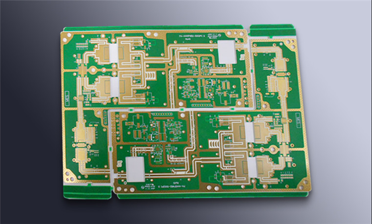
Laser Drilling Defects in PCB Microvia Fabrication
As conductor widths fall and pad pitches shrink, the mechanical drill reaches a limit. A bit that is small enough to produce a 0.15 mm hole is fragile, slow, and difficult to control to the depth required for a blind via. Laser drilling removed that limit by removing the cutting tool entirely, but it replaced a mechanical problem with an optical one, and the defects that appear on a laser-drilled HDI panel are different in kind from those seen on a mechanically drilled board.
Why Lasers Replaced Mechanical Drilling for Microvias
Build-up multilayer boards are made by adding dielectric layers onto a core and forming connections between them. The microvia that connects a new layer to the one beneath it is small, shallow and produced in large numbers, and it must land on a copper pad that is buried under the new dielectric. Mechanical drilling cannot do this reliably because the depth has to be controlled to within a fraction of the dielectric thickness and because the drill wears quickly at small diameters. A laser can be focused, pulsed and stopped at the copper beneath the dielectric, which makes it the natural tool for the job. The mechanism of material removal changes with the material, though, and that is the source of most of the process difficulty.
The Copper Window Method
The most common approach removes the dielectric through an opening in the copper foil, known as a copper window. The window is imaged and etched into the outer copper, and the laser removes the dielectric exposed inside it until it reaches the target pad underneath. The advantage is that the window also acts as a mask, limiting where the beam can remove material. The disadvantage is that everything now depends on the window and the target pad being in the right place relative to each other, and on the dielectric thickness under the window being uniform.
Registration Errors and Their Causes
Misalignment between the copper window and the target pad is the most common defect in this process, and it has several independent causes. The inner-layer artwork and the artwork used to open the window are produced on separate films, and both change dimension with temperature and humidity. The core expands and contracts during processing, and laminating the resin-coated foil onto it introduces a further dimensional shift. Etching the window adds its own tolerance in both size and position, and the laser system contributes an offset between the beam spot and the table position. Second-order blind vias, which land on a pad formed by an earlier build-up step rather than on the core, are harder still because the reference they must align to is itself the product of the previous step.
Practical countermeasures attack the largest contributors first. Reducing the panel size limits the absolute dimensional change across the panel; for boards with 0.10 mm lines and 0.15 mm blind vias, a working panel of about 350 mm by 450 mm is common. Increasing the beam diameter relative to the window gives the process more margin before the window is missed, and additional pulses can be added when the energy density is marginal. Opening the window slightly larger than the via means the hole position is no longer dictated entirely by the window edge, which allows the beam to be aimed at the target pad directly. Where the imaging and etching tolerance dominates, opening the window with a laser instead of by photolithography removes that contribution. For second-order vias, drilling alignment targets into the previous build-up layer and locating them with an X-ray system before drilling gives the process a reference that is closer to the feature being formed.
Incorrect Hole Shape
A hole that is wider at the bottom than at the top indicates that the beam is delivering more energy than the dielectric and the target pad can absorb evenly. This happens when the dielectric thickness varies across the panel, because a thinner region receives the same energy into less material and reflects more of it back into the wall. The result is a barrel-shaped opening that reduces the contact area between the plated copper and the target pad and weakens the connection. The cure has two parts: hold the dielectric thickness variation after lamination within a narrow band, typically a few micrometres, and adjust the energy density and pulse count using a designed experiment rather than a single trial, because the correct setting is a production condition and not a laboratory one.
Resin Smear and Desmear Quality
Laser drilling leaves residue on the target pad and on the via wall. If it is not removed, the plated copper bonds to the residue rather than to the copper beneath, and the connection fails later under thermal cycling. The removal step, desmear, must therefore reach every hole on the panel. That is difficult when a large panel carries tens of thousands of microvias and the dielectric thickness varies between them, because a single set of process conditions produces different residue levels across the panel. Tight control of the lamination thickness and a desmear process developed by experiment are the two levers available, and inspection after desmear should be done optically on a sample rather than assumed from the process settings.
Sidewall Erosion, Delamination and Fiber Protrusion
Several defects share the same root cause of excessive energy. Sidewall erosion appears when later pulses in a multi-pulse sequence reach a wall that has already been opened and reflect energy into it. Delamination between the copper window and the resin-coated foil occurs when the beam energy separates the two slightly. Fiber protrusion is specific to glass-reinforced dielectric, because the laser removes resin more readily than glass, leaving fibers standing proud of the wall. Residual resin that is not fully removed at the bottom of the hole, uneven energy absorption caused by panel warp, and micro-cracks at the edge of the target pad where reflected energy and heat damage the laminate all follow from the same imbalance between delivered energy and material thickness.
Process Control and Inspection
Because the defects are internal, control depends on measuring the process rather than the product. Dielectric thickness after lamination, window size and position after etching, beam energy and pulse count, and the target pad dimension should all be monitored as process parameters. Cross-sections on a sample basis confirm hole shape, wall quality and pad connection, and optical inspection after desmear catches residue that a cross-section might miss. Registration coupons placed at the corners and centre of the panel show how much the process drifts across the working area, which is the information needed to decide whether the panel size is the limiting factor.
Design Rules That Reduce Defect Rates
The layout can make the process easier or harder. Microvia diameters should sit comfortably inside the fabricator’s demonstrated capability rather than at its published minimum, and the target pad should exceed the via diameter by an annular margin that absorbs registration error. Stacked structures should be avoided where a staggered arrangement meets the electrical requirement, because each additional build-up step multiplies the alignment tolerance; the trade-offs are set out in this article on blind and buried via stack selection. Total board size and material choice also determine how much dimensional movement the process has to absorb, as described in this article on PCB dimensional stability, and the data preparation that supports these features is covered in this article on HDI board CAM methods.
FAQ
Why do laser-drilled microvias go out of registration? Usually because of dimensional movement between the inner-layer artwork and the window artwork, compounded by etching tolerance and beam-to-table offset. Reducing panel size attacks the largest contributor.
What causes a barrel-shaped microvia? Uneven dielectric thickness combined with fixed beam energy. The thinner region receives too much energy and the wall is driven outward.
Is residue on the microvia bottom a serious defect? Yes. Plated copper that lands on resin instead of the target pad forms a connection that may pass electrical test but fail under thermal cycling.