
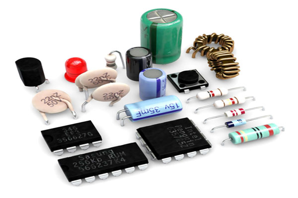
Via-to-Trace Spacing in Multilayer PCB Design Vias connect signals between layers, and their placement shapes what the fabricator can build. When routing density rises, vias crowd together and move closer to traces and copper pours. A clearance that looks fine in CAD may sit below what the drill, plating and…
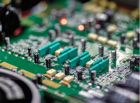
What Is a High-Reliability PCB? Reliability Explained A high-reliability PCB keeps its designed function across its full service life. It must survive electrical, thermal, mechanical and environmental stress without drifting outside specification. Passing a bare-board electrical test is not enough. The board must also support later assembly and stay stable…
Why High-Reliability PCB Manufacturing Matters A PCB that fails in the field costs far more than the board itself. Rework, warranty claims, downtime and lost reputation all trace back to process decisions made long before shipment. High-reliability manufacturing treats those decisions as engineering problems, not as luck. The goal is…
High-Current PCB Design: How to Prevent Board Burnout A board that burns out under load rarely fails without warning. The damage usually starts with a trace running too hot, a via carrying more current than it can handle, or a solder joint that slowly weakens under thermal cycling. High-current designs…
PCB Plated Hole Copper Thickness: Causes of PCB Failure A board can pass continuity testing and still fail in the field. The hidden cause is often thin copper on the wall of a plated hole. Plated holes carry current between layers, and they also absorb thermal and mechanical stress. When…
IPC Class 2 vs Class 3 PCB: Key Differences and Standards Two boards can leave the same shop with identical copper and still be judged by different rules. The IPC class decides which acceptance limits apply to holes, solder joints and surface features. It also shapes how much process control…
Pseudo 8-Layer PCB: Structure and Manufacturing Explained A pseudo 8-layer PCB looks like an eight-layer board in the stackup drawing. It routes signals on only six copper layers. The extra copper-clad core sits in the middle of the structure, and its copper is etched away completely. The board therefore carries…
PCB and PCBA Design Review Checklist for DFM and DFA A correct schematic does not guarantee a buildable board. Many failures appear only at fabrication or assembly, when a footprint disagrees with the BOM or a pad is too small. A structured design review catches these problems while changes are…
Single-Layer vs. Double-Sided vs. Multilayer FPC: Key Differences Flexible circuits carry a simple promise: connect components and route signals through a shape that bends. The layer count decides how much routing that shape can hold. A single copper layer suits simple interconnections. A double-sided build adds a second plane and…
PCB Panelization: 10 Critical Design Considerations Small boards are hard to hold, feed, and print. Panelization solves that by grouping several boards into one larger manufacturing format. The panel then travels through printing, placement, reflow, and inspection as a single unit. Good panel design keeps that unit rigid, aligned, and…