



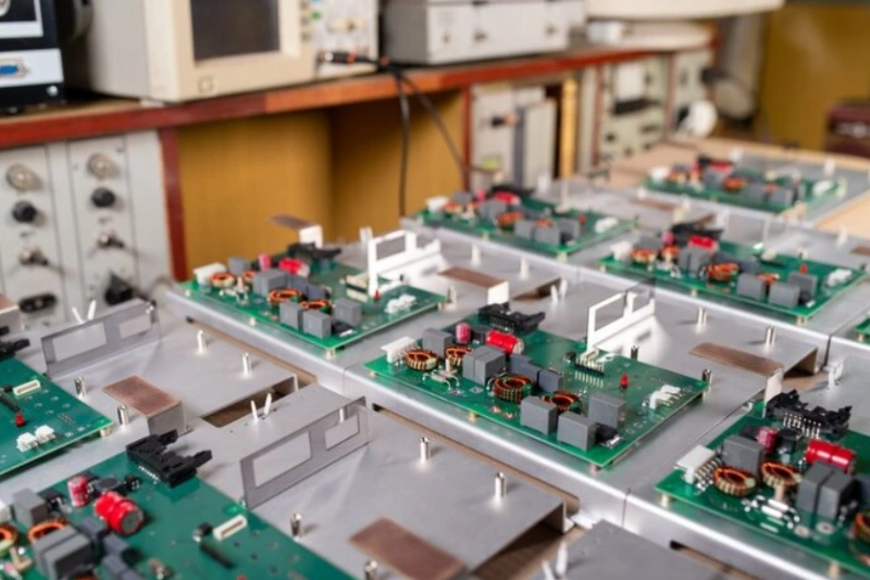
Blind Via PCB in Automotive Electronics: Design and Cost
Automotive electronics keeps getting more capable in a smaller volume, and the board has to keep up. Blind via PCB construction is one of the techniques that makes that possible: it allows a signal to move between layers without occupying the space that a through hole would need, which is exactly the constraint inside an engine control unit or a radar module.
What a blind via is
A blind via is a plated connection that reaches one outer layer and one or more inner layers, but stops before it passes through the board. It is the defining feature of many high-density interconnect designs, and it is what allows component density and routing density to rise without adding board area.
Unlike a through hole, which is visible from both sides, a blind via is open on one surface only, which is where the name comes from. It is produced by laser drilling followed by copper plating, and its depth has to be controlled closely because the same process must reach the intended layer without damaging the layers below.
Why automotive designs use them
The first reason is space. Systems inside a vehicle are packed tightly, and a board that can carry more routing per square millimetre can do more inside the same enclosure. In an engine control unit, where the volume is fixed by the mechanical design and the reliability requirement is severe, that density is what makes the design feasible at all.
The second reason is electrical. A blind via shortens the path a signal travels between layers, and a shorter path means lower inductance, less crosstalk, and a lower risk of electromagnetic interference. On a high-speed interface inside a safety-relevant module, those margins are worth paying for.
As vehicles adopt more high-density interconnect designs, blind vias provide the combination of performance, miniaturisation, and durability that the platforms require.
Where they appear
Advanced driver assistance systems are a natural fit, since radar, camera, and control modules combine limited space with a high layer count. Engine control units follow, because they need routing density, high-speed signal capability, and heat tolerance at the same time.
In-vehicle infotainment systems use them for high-resolution touch displays and audio and navigation subsystems that have to be compact. Battery management systems in electric vehicles use blind via construction to monitor and balance cells within a restricted volume, where the same feature also helps with heat spreading.
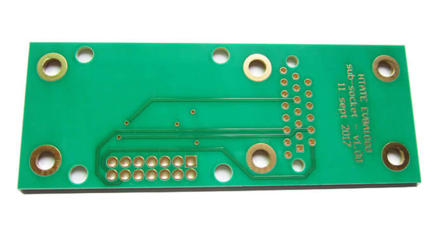
The value of a blind via is measured in millimetres of board area saved and in the signal integrity that the shorter path provides.
Design considerations
Material selection sets the thermal and mechanical foundation. Automotive designs commonly use a high glass transition temperature FR-4 or polyimide for thermal stability, with a metal substrate specified where heat spreading is the dominant requirement. The layer stackup is planned around signal integrity, power distribution, and impedance control rather than around the available copper.
Placing the blind vias is the detailed part. Each one has to avoid components, other holes, and keep-out areas while still making a reliable connection, and the depth has to sit inside the process window of the shop producing the board. Surface finish matters for the assembly process, and an immersion gold finish is often specified for solderability and oxidation resistance.
Compliance is a design input, not a final test. Automotive programmes typically work to an electronic component qualification standard, to a high-reliability PCB acceptance class, and to an automotive quality management system, and each of those requirements translates into layout and documentation decisions that are easier to satisfy when they are known at the start.
Advantages
Space saving is the most visible benefit, because blind vias raise component density without increasing board area. Signal integrity improves for the same reason, since shorter layer transitions reduce crosstalk and lower the risk of interference. Structural reliability benefits because replacing through holes with blind vias removes passages that would otherwise weaken the board and collect stress under vibration, and design flexibility increases because the routing is no longer constrained by barrels that pass through every plane.
Challenges
Manufacturing cost is the first challenge. Laser drilling, sequential lamination, and the additional inspection steps all add to the price of the board. Process difficulty is the second, since the depth of each hole has to be controlled precisely and the layer-to-layer registration has to hold across the whole panel.
Lead time is the third. More process steps take more time, and a design that depends on blind via construction should be scheduled with that in mind rather than quoted as if it were a routine multilayer board. Our guides to blind and buried via stack selection and to <a href="https://www.gopcba.com/electroplating-via-filling-hdi/” title=”electroplating and via filling in HDI”>electroplating and via filling in HDI cover the fabrication side of those decisions.

Blind vias are a capability purchase. The design is only feasible if the shop can hold depth control and registration on every panel, not on a sample.
What drives the cost
Layer count is the base of the calculation, because more layers mean more material and more processing. The number and complexity of blind and buried vias then adds to it, followed by the material grade, the surface finish, the order quantity, and the required delivery date. Certification requirements add their own share through additional testing and documentation.
Quantity has the largest single effect on unit price, because tooling and setup are fixed. Small orders and prototypes are therefore priced substantially higher per board than production volumes of the same design, which is why a prototype quotation should not be used to judge the production cost. Our guide to HDI board CAM methods explains how data preparation affects those costs before the first panel is produced.
Choosing a supplier
Not every fabricator can build automotive-grade blind via boards, and the questions that separate them are specific. Does the shop have experience with driver assistance, engine control, or electrified powertrain projects? Which quality systems and certifications apply to the process? Does it offer engineering review and cost optimisation rather than only accepting a data package? Does it run laser drilling, sequential lamination, and HDI processes in-house? And does its quality control include electrical test, X-ray inspection, and thermal cycling?
The answers determine both the reliability of the supply and the amount of engineering support available when a design has to be adapted, which is usually the difference between a smooth programme and a difficult one.
A note on documentation
Because a blind via is invisible from the outside, the fabrication drawing carries the whole specification: which layers each via connects, the depth tolerance, the surface finish, and the acceptance class. A drawing that describes the stackup only by layer count leaves the shop to infer the rest, and inference is where an automotive build goes wrong.
FAQ
When is a blind via worth the extra cost? When the alternative is a larger board, a thicker stackup, or a signal path that will not meet its integrity requirement. If a through via can do the job, it is cheaper and easier to manufacture.
Can blind vias be used in a rigid-flex automotive design? Yes, and the combination is common in compact modules, but the process becomes more involved because the flexible and rigid areas are laminated differently.
Do blind vias need special test coverage? They need the connections verified, which means electrical test with the appropriate probe access, plus X-ray inspection where the joint cannot be reached. Both requirements should be stated on the fabrication drawing.



1 Comment
ADAS System PCB: Design Requirements and Materials
[…] with HDI features, blind and buried vias, and fine-pitch escape routing from the processor. The blind via construction used to achieve that density adds lamination cycles and tightens registration […]