Custom Mechanical Keyboard PCB: Design and Assembly
A custom mechanical keyboard PCB is what separates a kit from a product. It connects the switches, the microcontroller, and the lighting, and it decides which layouts are possible, whether switches can be changed without a soldering iron, and how deeply the keyboard can be reprogrammed. Building one is a useful exercise in small-scale hardware design, because the project is simple enough to finish and detailed enough to teach.
What the board does
The board is the electrical centre of the keyboard. It connects the switches, the microcontroller, the indicating LEDs, and the connectors that carry data and power, and it is what allows the keyboard to recognise key presses and communicate them to a computer.
Unlike a membrane keyboard, which uses a rubber dome and a printed contact sheet, a mechanical board uses an individual switch for every key. That difference produces a longer service life, a more consistent feel, and a much greater ability to be customised.
How the circuit works
Each key is a switch that closes a circuit when it is pressed. The board routes that circuit to the microcontroller through copper traces, and the microcontroller converts the event into a key code that the computer understands.
Three details are worth understanding before designing or repairing one. The copper traces are the signal paths between each switch position and the controller, so their routing determines how the matrix is organised. The diode at each switch position prevents signal interference between keys and is what enables simultaneous key registration. And the way the microcontroller is connected determines which firmware will run on the board and which features are available.
Mechanical and membrane boards compared
The switch type is the visible difference: discrete mechanical switches against a rubber dome. Durability follows from it, since a mechanical switch is rated for tens of millions of actuations while a membrane contact wears much sooner.
Customisation is the third difference and the one that matters for a custom build. A mechanical keyboard PCB can be remapped in firmware, which means the same hardware can present a different layout, and it can support multiple layers so that one key performs several functions depending on the layer that is active.

Firmware is where a custom keyboard earns its name. The layout is a decision, not a property of the hardware.
Features to decide before layout
The switch interface is the first decision. A hot-swap socket lets switches be replaced without soldering, which is what makes a board a long-term platform; a soldered build provides a more permanent connection and a lower profile. Compatibility matters here as well, since switches come in three-pin and five-pin variants and the board has to accept the one that will be used.
Programmability is the second decision. Firmware such as QMK firmware runs on the controller and gives the board its layer system, macros, and remapping, and configuration tools allow the keymap to be changed without recompiling. Illumination is the third: per-key backlighting and underglow are separate features, and both are driven from the firmware rather than from dedicated hardware.
Design decisions
Layout comes first, and it is a working decision rather than an aesthetic one. A compact 60 percent layout saves desk space and shortens the matrix; a full-size board adds keys and therefore more routing. Ergonomic formats such as a split or an angled design change the mechanical design as much as the electrical one, and any layout that uses macros or function layers should be planned before the matrix is drawn.
The microcontroller choice follows the required features. Compatibility with the intended firmware is the first filter, power consumption is the second for wireless designs, and expandability is the third for boards that will carry a small display or a rotary encoder. Connectivity completes the picture: a USB-C connector is the default for durability and data rate, while a wireless design needs a battery and charge management integrated into the same board.
Fabrication and assembly
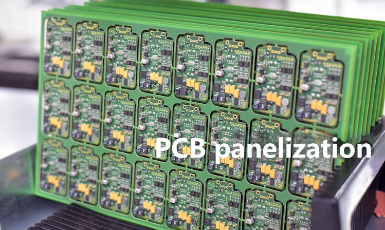
The board is designed in standard electronic design automation software, with the switch footprints, diodes, and controller placed and routed before the fabrication data is generated. Fabrication then follows a normal process, and the assembly sequence is what most builders underestimate.
The order that works is consistent: clean the board, fit and solder the diodes while the surface is still accessible, then the switches and any lighting, and finally the controller. Each step is easier when the larger parts are not yet in the way, which is the same reasoning that governs placement order on any assembly. The general principle is covered in our guide to placement order and pad positioning.
Assembly order is not a preference. It is the difference between a board that can be repaired and one that has to be rebuilt.
Firmware and configuration
Flashing firmware requires the board to enter its bootloader mode, which is normally done by holding a defined key while connecting the cable. The firmware image is then loaded through the flashing tool, and the keymap and macros are configured afterwards.
Keeping the configuration under version control is worth the small effort, because the keymap is part of the design. A layout that exists only on one computer is a layout that will be lost the first time the machine is replaced.
Testing and troubleshooting
Testing starts with continuity. A multimeter in continuity mode confirms that each switch position connects when pressed and that no neighbouring positions share a connection. That single check catches most assembly faults before power is applied.
Three faults cover the rest. A key that does nothing usually points to a solder joint or to a diode fitted the wrong way round, since the diode is what prevents signals from one key interfering with another. Firmware that will not load usually means the board never entered bootloader mode. And key conflicts, where several keys register incorrectly when pressed together, point to diode orientation and to whether simultaneous key registration is enabled in the firmware.
Where the board ends and the case begins
The board has to fit the case, and the case has to clear the sockets, the connector, and any switch that sits close to the edge. Deciding the mounting holes, the stabiliser positions, and the plate clearance together with the electrical layout prevents the most common late change on a keyboard project, which is moving a component because the enclosure would not close.
FAQ
Is a custom keyboard PCB expensive to build? The board itself is usually a simple two-layer design and costs little. The expense, if any, is in the number of revisions, which is why testing the matrix on a first prototype before finalising the layout is worthwhile.
Should I use a hot-swap socket or solder switches directly? Hot-swap for a board that will be used and modified over time, and direct soldering for a build that will not change. The socket adds a small amount of height and cost.
How many layers does a keyboard PCB need? Most designs work on two layers. A four-layer board becomes attractive when the matrix is large, when lighting is distributed across the board, or when the traces have to pass around a controller in the centre. Background on the wider assembly flow is available in our guide to the PCBA development process, and the placement problems that a large component count creates are described under SMT component shift causes.