
Blind and Buried Vias: Density Without Dead Layers
Blind and buried vias exist because a through hole occupies every layer it crosses. On a dense board the through holes themselves become the limiting factor: they block routing channels on inner layers, they force the escape pattern of every large device, and they leave unused stubs that degrade a high speed signal. Restricting a connection to the layers that actually need it recovers that space.
The price is sequential lamination. Each pair of layers that has to be drilled before the next lamination adds a cycle, and each cycle adds registration error, cost and lead time. Choosing where to spend those cycles is the design decision that follows from the stackup, not from the drill chart.
What Each Via Type Costs and Buys
A buried via connects inner layers only and is invisible after lamination, so it can sit directly under a component without disturbing the surface. A blind via reaches the surface, which makes it useful for escape routing but also means its annular ring and its capping have to survive assembly. Both free the layers above and below that a through hole would have blocked.
The benefit is easy to overstate. If the routing density is low, a through hole costs nothing and the added lamination cycles are pure expense. The technique pays where several dense devices sit close together and their escape patterns compete for the same inner layers, which is the situation described in the discussion of high density interconnect boards.
Sequential Lamination and Registration
Registration is the capability that decides how many sequential cycles are practical. The inner layers of a sub assembly are drilled after they are bonded, and the panels must then be laminated at least once more with the outer layers, all while keeping the drilled features within a tolerance that allows the next connection to land on them.
Stacked via structures multiply that problem, because each via has to sit on the one below it within a fraction of the pad diameter. Where the registration window is tight, a staggered arrangement, in which each via lands on a small pad rather than directly on the one beneath, gives the process room to breathe at the cost of a little more area.
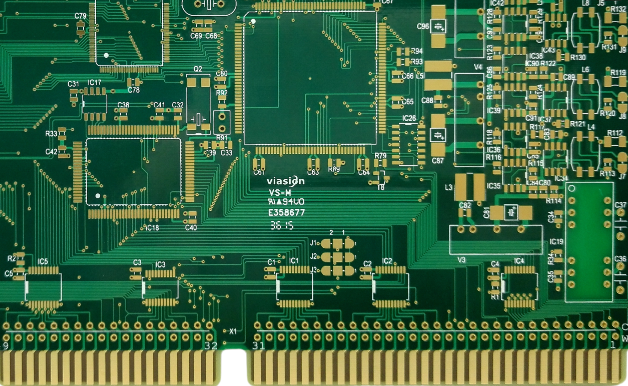
Aspect Ratio and Drill Limits
A blind via is drilled from the surface to a depth set by the lamination, so its aspect ratio is the depth divided by the drill diameter. That ratio, not the total board thickness, is what limits the process, and it is why a thin sub assembly can carry a via that would be impossible through the finished board.
The practical limits follow from plating. Chemistry has to reach the bottom of the hole and copper has to be deposited evenly along a barrel that may be only a few times its own diameter long. Where the ratio is pushed, the plating thins at the middle of the barrel and the connection becomes a reliability risk that only a thermal cycle test will expose.
Designing the Annular Ring and Pad
Every drilled feature needs a capture pad large enough to absorb the registration error of the process that will connect to it. On a blind via the pad has to survive both the drilling tolerance and the lamination shift, so it is usually larger than the designer expects. Reducing it to gain routing space is a common mistake that shows up as an open barrel rather than as a short.
Where the pad cannot grow, the honest options are to reduce the number of sequential cycles or to choose a different escape strategy. Fabrication notes should carry the drill sizes, the tolerances and the layer pairing explicitly, in the form used for a fabrication notes package, because a supplier left to interpret a stackup will optimise for the cost of the quotation.

Electrical Consequences
Removing the stub is the electrical reason to use a buried via on a high speed net. A through hole that passes the connection point and continues to the far side of the board leaves a resonant stub, and the resonance shows up as a notch in the insertion loss at a frequency set by the stub length. A buried via simply does not have one.
Blind vias still carry a short stub from the surface to the target layer, so the benefit is partly the shorter length and partly the extra routing freedom. On differential pairs the two vias of a pair should be arranged symmetrically, because an asymmetry in length or in the surrounding copper turns into a mode conversion that no amount of matching will remove.
When a Through Hole Is the Right Answer
Through holes are cheaper, stronger in a thermal sense, and much easier to inspect, because a barrel can be seen from both ends. On a board with moderate density, or one that will be exposed to repeated thermal cycling in a harsh environment, the additional reliability margin of a fully plated through hole is worth more than the routing space.
A mixed approach usually works best: keep through holes for power, ground and anything that carries heat, and reserve the blind and buried structures for the high speed nets and the fine pitch escapes that genuinely need them. That division keeps the number of lamination cycles down, which keeps both the cost and the yield risk under control, as discussed in the wider review of PCB manufacturing processes.
Additional Considerations for This Build
Practical attention to via density pays for itself here, because it decides whether the finished board behaves as the drawing intended. Where the requirement is not stated on the fabrication drawing or in the assembly notes, the shop has to assume a default, and that default is rarely the value the design was simulated with. Stating via density explicitly, together with the tolerance that applies, removes the assumption and keeps the result predictable from batch to batch.
Process Control and Verification
On a design of this kind, via density is the item that decides how the rest of the board is arranged. The process window is set by the narrowest step in the flow, so an improvement anywhere else shows up as margin rather than as yield until that step is addressed. A short note on the drawing about handling, storage or packaging is often worth more than an extra decimal place on a tolerance.
Where a value sits close to a process limit, the drawing should say so, since the shop can then open the process window rather than working to a nominal figure that carries no tolerance.
FAQ
How many sequential lamination cycles are realistic? Most volume products stop at two or three. Each additional cycle adds registration error and cost, and beyond that point an any layer or HDI approach is usually the better route.
Can a blind via be used under a ball grid array? Yes, and it is a common escape technique. The surface still has to be flat and capped, so the plating and planarity specification applies as it does to any pad that will be soldered.
Do buried vias need to be tested? They cannot be probed directly from the surface, so the net is verified through the components connected to it or by a fixture that reaches the accessible ends of the chain.