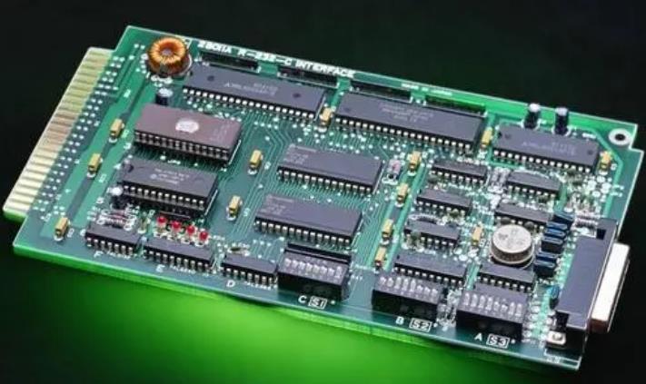
PCBs With Blind and Buried Vias: Design and Applications
A through hole is the simplest interconnect in a printed circuit board and, on a dense design, also the most wasteful. It occupies a footprint on every layer it passes through, whether or not it connects anything there, and a cluster of them under a large package can carve a ground plane into disconnected pieces. Blind and buried vias exist to remove that waste.
What Blind and Buried Vias Are
A blind via connects an outer layer to one or more inner layers without passing through the whole board. It is called blind because it cannot be seen from the opposite side. On a six layer board, a via that links layer one to layer two is blind, and it is the standard way to escape a dense package without drilling through the ground plane below.
A buried via connects two or more inner layers and never reaches either outer surface, so it is completely hidden inside the finished board. A via linking layer two to layer three on a six layer stackup is buried. Both types are formed before the outer layers are laminated, which is why they are confined to the inner portion of the stackup.
Why They Are Used
Space is the first reason. Because a blind or buried via does not consume a footprint on every layer, the layers it does not touch remain available for routing or for a continuous reference plane. That allows a design to be more compact or to use fewer layers for the same function, and both outcomes reduce cost when the layer count is the dominant cost driver.
Signal integrity is the second reason. A shorter via barrel has less series inductance and less parasitic capacitance, so it distorts the signal less and creates a smaller stub below the connection point. At high frequency the stub is what limits performance, since it resonates and produces a notch in the insertion loss, and shortening or eliminating it is the main electrical benefit of the technology.
Layer Stackup Planning Comes First
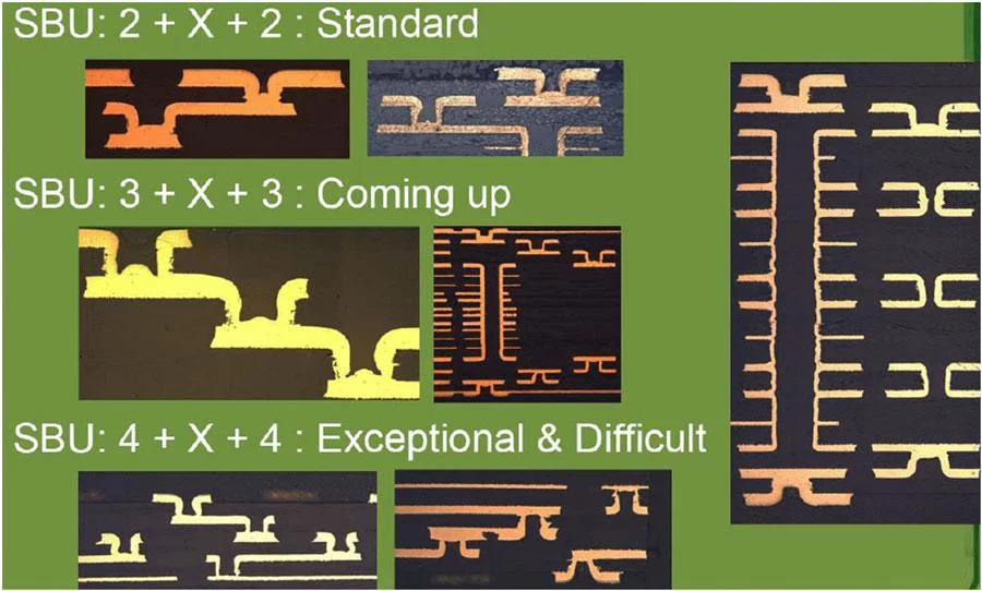
Blind and buried vias are defined by the stackup, so the stackup has to be planned before routing begins. Each sequential lamination step adds a pair of layers and a set of vias between them, so the stackup determines how many lamination cycles the board needs and therefore what it will cost. A one time build with one lamination cycle is far cheaper than a three time build.
The mechanical drilling and laser drilling requirements also follow from the stackup. A laser drilled microvia can only be formed through a thin dielectric, typically 0.1 mm or less, so the layer construction has to place the thin dielectric exactly where the microvias are needed. Attempting to add blind vias to a stackup that was designed for through holes usually means rebuilding the entire layer arrangement.
Sizing and Placement Rules
Via diameter has to balance space saving against manufacturability. A smaller via consumes less area but requires a finer drilling process and a plating chemistry that can reliably coat a high aspect ratio barrel. The aspect ratio, the ratio of board thickness to drilled diameter, is the number that governs plating reliability, and pushing it too high is the most common cause of a failed buried structure.
Vias must also be kept apart. Placing blind vias too close together creates a local concentration of resin starved laminate during pressing, which shows up as delamination or as voiding in the barrel. As a working rule, spread the vias across the board, fill unused ones, and check the fabricator recommendation for minimum pitch at the via size being used.
Material Choice
The laminate has to survive the additional drilling and lamination steps, so dimensional stability and resin flow behaviour matter more than they do on a through hole board. A material that moves during pressing will misregister the inner layers against the microvia, and the resulting non-conformance is invisible until electrical test. Low flow or no flow prepreg systems are often specified for this reason.
Where the design also carries high frequency signals, the laminate selection becomes a loss and dielectric constant problem rather than purely a mechanical one, and the two requirements have to be satisfied by the same material. That limits the options, so the choice belongs in a design review with the fabricator rather than in a purchase order.
Manufacturing Sequence
Buried vias are created first. The inner layers are imaged and etched, the buried vias are drilled and plated, and those layer pairs are laminated together and then pressed into the growing stackup. Blind vias come later, usually formed by laser drilling into the outer films after the inner core is complete, which is why they can only reach the first few layers.
Plating then connects the barrels, and the sequence repeats for each additional lamination cycle. Inspection is heavier than on a conventional board: X-ray is used to check registration of the buried features and automated optical inspection to verify the outer layers. The laser process and its limits are described in electroplating and via filling for HDI.
Advantages and Applications
Beyond density, the advantages are design flexibility and reliability. Fewer through holes means fewer places where a barrel can crack under thermal cycling, and the ability to route on inner layers without obstruction allows better optimisation of return paths and thermal copper. The shorter barrels also reduce the number of potential failure sites in the interconnect.
The applications follow from that combination. Smartphones, tablets and wearables need both density and low loss. Medical imaging and implant equipment need reliability and signal integrity. Avionics, satellites and defence systems need all of the above plus documented process control, and automotive radar and infotainment modules need high density with the thermal cycling tolerance of a vehicle environment. Server and accelerator boards use the technique to support very high speed links.
Cost and Lead Time
The penalty is real. Sequential lamination multiplies the number of process steps, laser drilling is slower than mechanical drilling, and inspection has to be more thorough because a defect inside a buried layer cannot be reworked. Lead time extends for the same reasons, and a board with three lamination cycles cannot be turned around as quickly as a through hole design.
The design effort also rises, because the stackup, the via types and the routing strategy have to be settled together rather than in sequence. Compound that with the requirement that the fabricator has the equipment and experience for the construction, and the technology becomes a decision to be planned rather than an option to be added late. Related constructions are compared in via in pad or plated through.
FAQ
Can blind and buried vias be combined on one board? Yes, and they usually are. A buried via forms the inner connection during the first lamination cycle, and a blind via reaches the outer layer afterwards. Each additional type and lamination step adds cost, so the mix should be justified layer by layer.
Are microvias the same as blind vias? Not quite. A microvia is defined by its size and by being laser drilled, and it is normally a blind via. A blind via can also be mechanically drilled at a larger diameter, which is cheaper but consumes more space and has a longer barrel.
How much height does a buried via save? It saves board area rather than height. Because the barrel does not pass through the layers above and below, those layers keep their routing area and their reference plane, which is what allows a denser escape in the same outline, following the rules in blind and buried via stack selection.