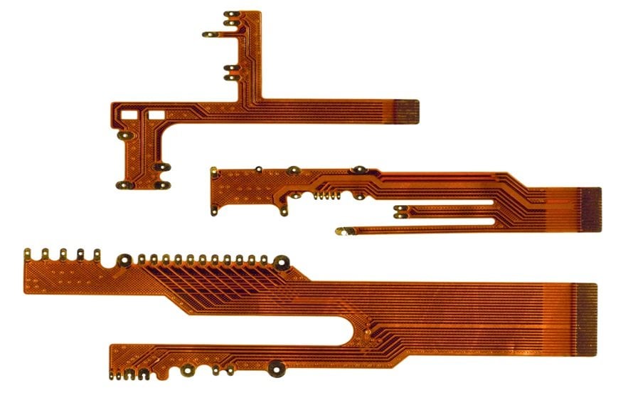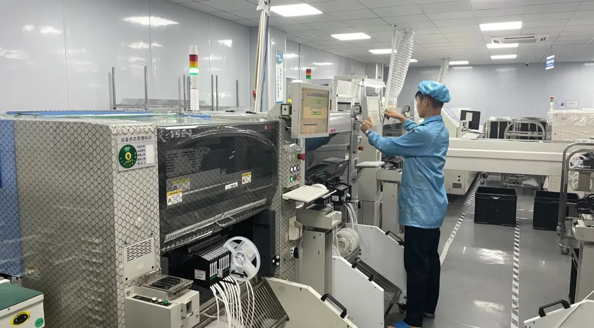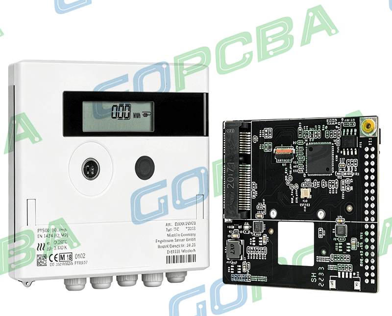
PCB In-circuit Test Node Access: Reaching Every Net Modern electronics depend on boards that are assembled correctly the first time. Every product – a phone, a charger, a medical instrument or an industrial controller – relies on thousands of solder joints that must conduct current for years. This article explains…
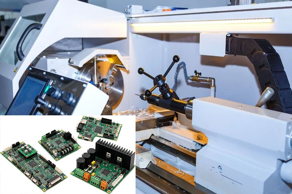
PCB Functional Test Setup: Exercising the Whole Product Electronics manufacturing has become a discipline of small details. Solder paste volumes, placement accuracy, temperature profiles and inspection limits all add up to the final result. This guide looks at PCB functional test setup from the perspective of a PCBA factory floor,…
PCB Golden Board Comparison Test: Checking Against a Known Good Electronics manufacturing has become a discipline of small details. Solder paste volumes, placement accuracy, temperature profiles and inspection limits all add up to the final result. This guide looks at PCB golden board comparison test from the perspective of a…
PCB 3D AOI for Paste Height: Measuring the Paste in Three Dimensions Buyers and engineers often focus on the finished product and forget the production line behind it. In practice, most field failures can be traced back to process decisions made during assembly. Understanding PCB 3D AOI for paste height…
PCB AOI Programming: Teaching the Machine to Look Modern electronics depend on boards that are assembled correctly the first time. Every product – a phone, a charger, a medical instrument or an industrial controller – relies on thousands of solder joints that must conduct current for years. This article explains…
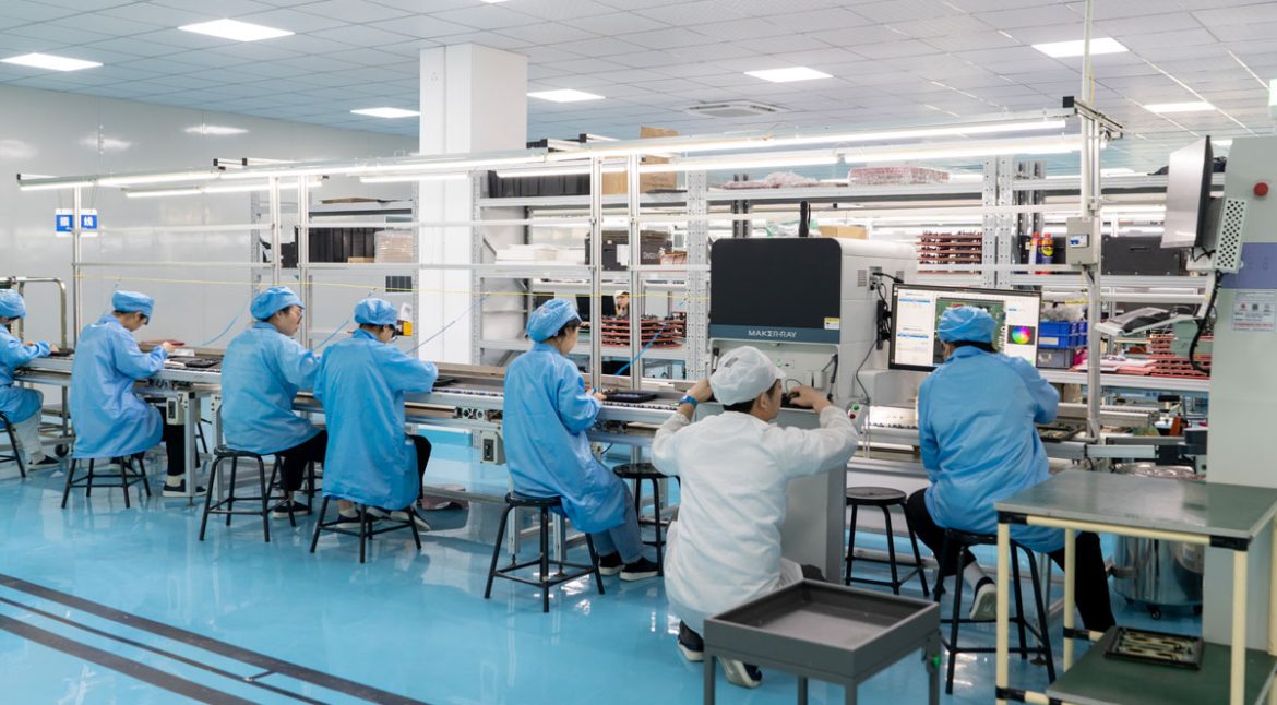
PCB CT Scan for Solder Joints: A View from Every Angle Buyers and engineers often focus on the finished product and forget the production line behind it. In practice, most field failures can be traced back to process decisions made during assembly. Understanding PCB CT scan for solder joints gives…
PCB X-ray Inspection of BGA Voids: Seeing Inside the Solder Modern electronics depend on boards that are assembled correctly the first time. Every product – a phone, a charger, a medical instrument or an industrial controller – relies on thousands of solder joints that must conduct current for years. This…
Land Pattern Errors: Why Pads Spaced Too Far Apart Fail in Reflow Most footprint errors are obvious once they are pointed out: a pad that is too short, a wrong pin numbering, a missing thermal pad. The one that causes the most trouble in production is more subtle. It is…
PCB Short Circuit: Finding and Preventing the Ones That Escape A short circuit on a finished board is expensive because it usually appears after the material and the assembly time have been spent. The causes are few and well understood, which means most of them can be designed out and…
Layer Change or Detour: Choosing Between a Via and a Bend The question comes up on almost every high speed layout: is it better to change layer through a via, or to stay on the same layer and route around the obstacle? The two options trade one discontinuity for another,…