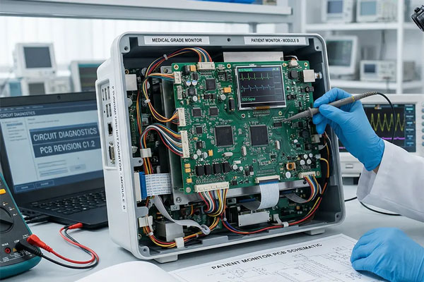
PCB Placement Clearance Design: Room Around Every Part Buyers and engineers often focus on the finished product and forget the production line behind it. In practice, most field failures can be traced back to process decisions made during assembly. Understanding PCB placement clearance design gives you a practical advantage when…
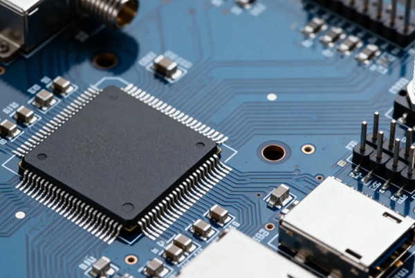
PCB Panel Edge Clearance: Keeping Copper Away From the Cut Modern electronics depend on boards that are assembled correctly the first time. Every product – a phone, a charger, a medical instrument or an industrial controller – relies on thousands of solder joints that must conduct current for years. This…
PCB Drill Tool Wear Monitoring: Watching the Bit Cut Buyers and engineers often focus on the finished product and forget the production line behind it. In practice, most field failures can be traced back to process decisions made during assembly. Understanding PCB drill tool wear monitoring gives you a practical…
PCB Gerber Data Package: The Files the Factory Needs Buyers and engineers often focus on the finished product and forget the production line behind it. In practice, most field failures can be traced back to process decisions made during assembly. Understanding PCB gerber data package gives you a practical advantage…
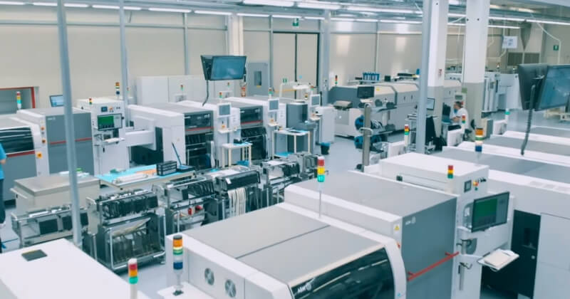
How to Choose the Right SMT PCB Assembly Manufacturer For hardware developers, completing the PCB design and sourcing components are only part of the manufacturing process. The next critical step is assembly. The quality of surface-mount assembly directly affects product yield, reliability, and long-term performance. Problems such as solder…
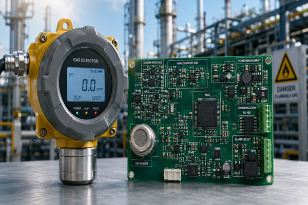
How to Choose anIndustrial PCBA Control PCB Partner Industrial control electronics have very different requirements from consumer products. A control board may need to operate continuously for years while facing temperature changes, vibration, electrical noise, humidity, and other demanding conditions. For this reason, industrial electronics development should not focus…
PCB Engineering Question Management: Asking Before the Build Electronics manufacturing has become a discipline of small details. Solder paste volumes, placement accuracy, temperature profiles and inspection limits all add up to the final result. This guide looks at PCB engineering question management from the perspective of a PCBA factory floor,…
PCB Via Plating Thickness: Copper Inside the Hole Modern electronics depend on boards that are assembled correctly the first time. Every product – a phone, a charger, a medical instrument or an industrial controller – relies on thousands of solder joints that must conduct current for years. This article explains…
PCB Stencil Underscreen Wiping: Cleaning the Foil Between Prints Buyers and engineers often focus on the finished product and forget the production line behind it. In practice, most field failures can be traced back to process decisions made during assembly. Understanding PCB stencil underscreen wiping gives you a practical advantage…
PCB High Voltage Clearance: Space Between Live Conductors Buyers and engineers often focus on the finished product and forget the production line behind it. In practice, most field failures can be traced back to process decisions made during assembly. Understanding PCB high voltage clearance gives you a practical advantage when…