PP thickness

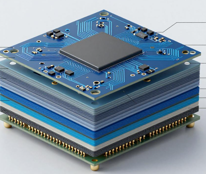
PCB Stackup Optimization: Using Copper Distribution to Reduce PP Thickness

When engineers calculate dielectric thickness in a multilayer PCB stackup, the primary focus is often target impedance. However, the physical topography created by etched inner-layer copper is equally important. After inner-layer etching, copper-covered areas and resin-filled areas do not have the same surface height. During lamination, the resin in prepreg…

PCB file revision control

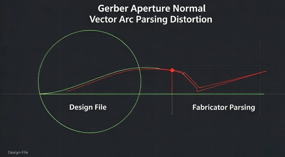
PCB File Revision Control: Preventing Production Errors and Rework

In PCB manufacturing, prototype development is often accompanied by multiple rounds of design optimization. Engineers may adjust component placement, routing, layer stackup, impedance parameters, hole dimensions, materials, or manufacturing processes after each prototype build. These changes are normal during product development. The real risk occurs when updated design files, manufacturing…
Wire Harness

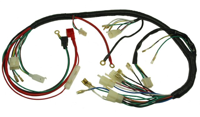
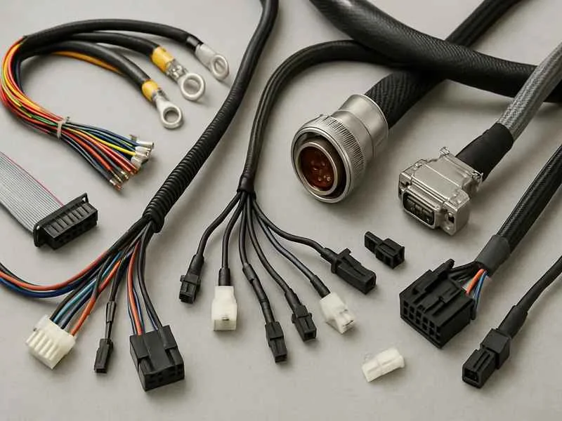
Wire Harness: Components, Types, Materials & Manufacturing

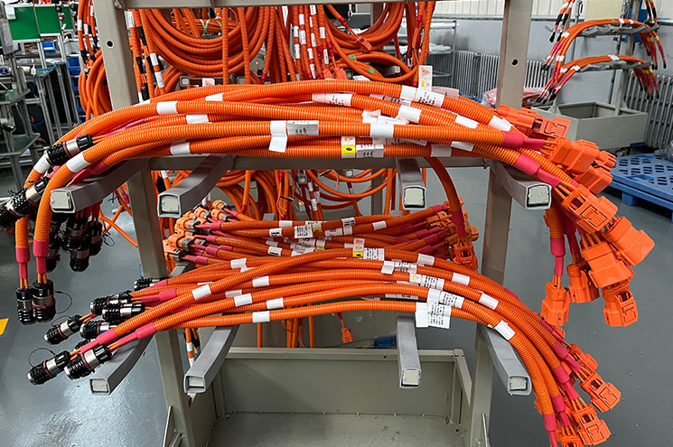
A wire harness is an engineered electrical assembly that organizes multiple wires, terminals, connectors, and protective components into a defined routing structure. By integrating individual conductors into a pre-assembled unit, a wire harness simplifies installation, improves wiring consistency, and supports reliable power and signal transmission inside electronic and electrical equipment.…
PCB impedance

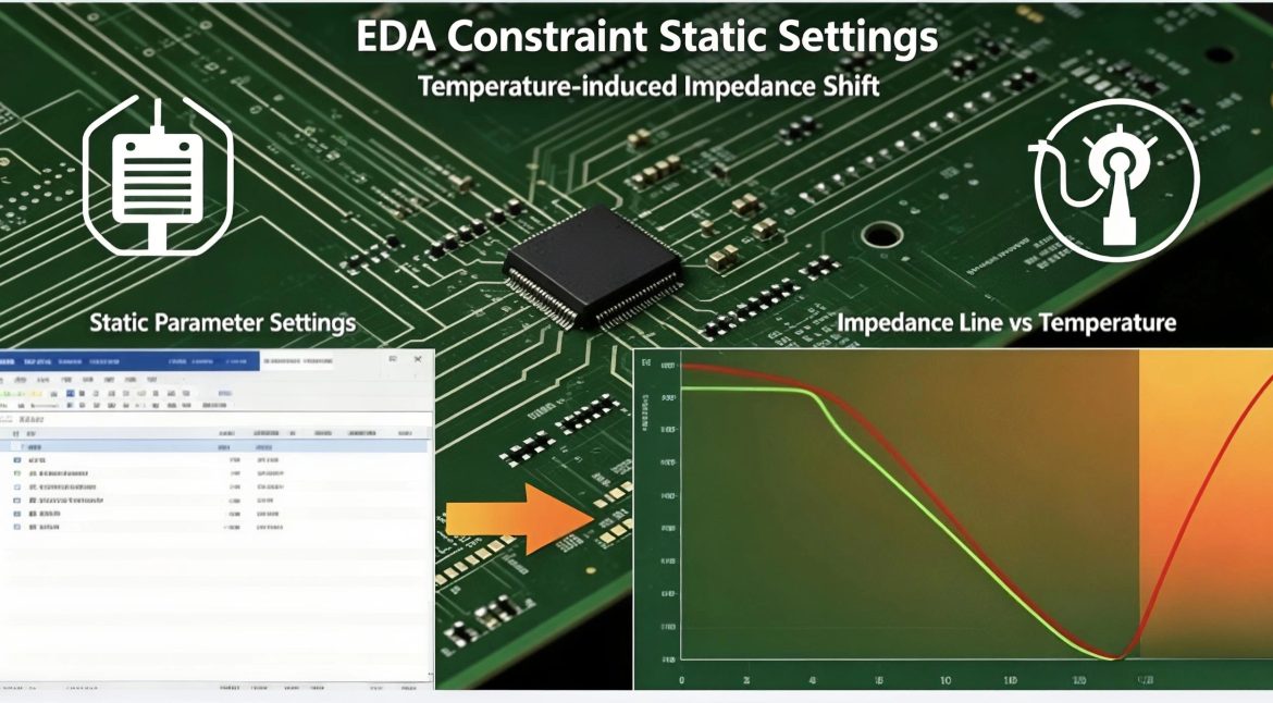
Temperature-Dependent PCB Impedance: EDA Constraints for High-Speed Design

In high-speed PCB design, impedance control is often established through a fixed set of parameters in the EDA environment. Designers typically define target impedance, dielectric thickness, copper thickness, trace width, trace spacing, and dielectric constant at a nominal temperature. This approach may work adequately for products operating near room temperature.…