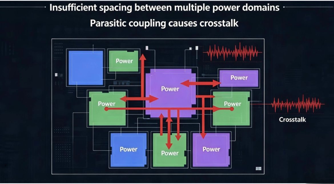
In mixed-signal PCB designs, digital and analog power domains often operate close to each other. When high-speed digital power such as VCC_IO is routed or poured near sensitive analog rails such as VDDA, unwanted noise can be transferred through parasitic capacitance, shared impedance, return-path discontinuities, and electromagnetic coupling.
This problem can be particularly noticeable in ADCs, DACs, PLLs, RF circuits, sensor interfaces, and precision measurement systems.
A PCB may pass basic electrical testing and still exhibit excessive noise after the complete system is powered up. In many cases, the problem is not simply caused by an LDO, regulator, or decoupling capacitor. The physical structure of the PCB itself can create an unintended coupling path between power domains.
Therefore, power domain spacing should be treated as part of the overall power-integrity and signal-integrity design strategy rather than simply as a clearance rule.
A Typical Mixed-Signal PCB Failure
Consider a four-layer industrial control board containing a 3.3 V digital power domain, VCC_IO, and a 1.8 V analog supply, VDDA.
If both power regions share the same top-layer copper area and the separation between their boundaries is very small, high-frequency switching currents from the digital domain can couple into the analog domain.
The resulting symptoms may include:
- Increased ADC noise floor
- Periodic noise spikes in sampled data
- Additional spectral peaks
- Reduced effective number of bits (ENOB)
- Increased PLL or clock jitter
- Unstable sensor measurements
- Unexpected noise on analog reference rails
For example, a switching component around 100–200 MHz can appear on an analog supply even when the regulator itself has adequate nominal performance.
The correct troubleshooting question is therefore not simply:
“Is the LDO working correctly?”
It should also be:
“What coupling path allows the digital switching current to reach the analog power domain?”
Why Capacitive Coupling Occurs Between Power Domains
One of the most important mechanisms is capacitive coupling.
Whenever two conductive structures are separated by a dielectric material, they form a parasitic capacitance. On a PCB, this can occur between:
- Adjacent copper regions
- Parallel power traces
- Copper planes on neighboring layers
- Pads and nearby copper
- Via structures
- Copper regions separated by solder mask or laminate
A simplified capacitance relationship is:
[C_p \approx \frac{\varepsilon_r\varepsilon_0 A}{t}]
where:
- (C_p) is the parasitic capacitance
- (\varepsilon_r) is the effective relative dielectric constant
- (\varepsilon_0) is the permittivity of free space
- (A) is the effective overlapping area
- (t) is the dielectric separation
This relationship shows why both spacing and geometry matter.
However, the simple parallel-plate equation does not fully describe two copper regions placed side by side on the same PCB layer. In that case, electric-field fringing becomes important, and the effective capacitance depends strongly on:
- Copper geometry
- Edge-to-edge spacing
- Dielectric thickness
- Material properties
- Reference-plane geometry
- Copper overlap
- Frequency
Therefore, the calculation should be considered an engineering approximation rather than an exact prediction of real-board coupling.
High dv/dt Creates Larger Coupling Currents
The current through a parasitic capacitor can be approximated by:
[I_c=C_p\frac{dV}{dt}]
This equation is particularly important for high-speed digital circuits.
A digital signal with a relatively low voltage swing can still generate significant high-frequency coupling if its transition time is extremely short.
For example, a signal with a 1 V/ns edge rate contains substantial high-frequency spectral content even if its fundamental clock frequency is much lower.
This means that PCB noise should not be evaluated only from the nominal switching frequency.
The dv/dt of the switching waveform is often more important when evaluating capacitive coupling.
As power domain spacing decreases and the effective coupling area increases, the parasitic capacitance can increase, allowing more displacement current to enter nearby structures.
Why PCB Crosstalk Is Not Determined by Distance Alone
It is tempting to treat spacing as the only parameter controlling PCB crosstalk.
In reality, coupling depends on several variables simultaneously.
For capacitive coupling, the major factors include:
- Electric-field strength
- Edge rate
- Coupled area
- Dielectric thickness
- Relative permittivity
- Source impedance
- Victim impedance
- Return-path structure
For inductive coupling, current-loop area and mutual inductance become important.
For power networks, common impedance coupling can also become significant when multiple circuits share:
- Vias
- Plane regions
- Copper necks
- Ferrite beads
- Decoupling paths
- Ground return structures
Therefore, simply increasing the distance between two power traces may not completely solve a noise problem if the two domains still share a poorly controlled return path.
Power Domain Spacing Must Be Evaluated With Three Constraints
A practical mixed-signal PCB layout should evaluate at least three areas.
1. Electric-Field Coupling
The first consideration is power domain spacing.
A small clearance increases the possibility of electric-field coupling, particularly when the adjacent domain contains fast voltage transitions.
However, there is no universal spacing value that guarantees immunity from crosstalk.
A spacing such as 0.15 mm may be acceptable for one low-speed application but inappropriate for another design containing high-speed switching edges and highly sensitive analog circuitry.
Instead of adopting one fixed value for every design, engineers should consider:
- Edge rate
- Coupled length or area
- Layer structure
- Dielectric thickness
- Sensitive-node impedance
- Noise tolerance
For sensitive analog supplies, increasing physical separation is usually only one part of the solution.
2. Reference-Plane Continuity
The second constraint is reference-plane integrity.
A sensitive analog power region should have a predictable return-current environment.
If the reference plane beneath a high-speed digital region is interrupted, return current may be forced to travel around the discontinuity.
This increases loop area and can increase inductive coupling.
A common mistake is to separate power regions while simultaneously creating unnecessary gaps in the underlying ground plane.
The result can be counterproductive:
Power-domain separation improves, but return-path integrity becomes worse.
For this reason, PCB layout should be evaluated layer by layer rather than looking only at the top-layer copper pattern.
3. Power-Distribution Impedance
The third constraint is power integrity.
Even if two power domains are physically separated, they can still interact through:
- Shared ground impedance
- Common vias
- Regulator output impedance
- Ferrite beads
- Plane connections
- Decoupling capacitors
The resulting noise voltage can be approximated conceptually as:
[V_{noise}\approx I_{noise}Z_{path}]
This explains why reducing the coupling current alone may not be sufficient. The impedance of the receiving power network also matters.
Do Not Assume a Copper Strip Is a Shield
One of the most common layout mistakes is placing a narrow floating copper strip between two power domains and assuming that it acts as an electromagnetic shield.
A floating copper structure can become another parasitic element rather than an effective shield.
For high-frequency isolation, a grounded guard structure can sometimes be useful, but its effectiveness depends on:
- Connection to the ground network
- Via placement
- Geometry
- Frequency
- Return-current distribution
- Nearby reference planes
A guard trace should therefore be designed as part of the complete return-current structure.
Simply inserting an unconnected copper strip does not guarantee improved isolation.
Ground Guarding and Via Placement
When a grounded guard trace is appropriate, stitching vias can help maintain a low-impedance connection to the reference plane.
The commonly cited rule of placing stitching vias at a fraction of the signal wavelength can be useful as an initial guideline, but it should not be treated as a universal requirement.
At high frequencies, the relevant wavelength depends on the propagation medium and effective dielectric constant rather than simply the speed of light in free space.
For example, for a 125 MHz noise component, the free-space wavelength is approximately 2.4 m. The guided wavelength on a PCB is shorter and depends on the effective dielectric constant.
More importantly, the dominant coupling mechanism should be identified before selecting a via pitch.
If the problem is mainly common impedance coupling, simply adding more ground vias may not address the root cause.
Material Dk Also Affects Parasitic Capacitance
PCB dielectric properties influence electric-field coupling.
A simplified relationship shows:
[C\propto\varepsilon_r]
Therefore, a material with a lower effective dielectric constant can produce lower capacitance for an otherwise similar geometry.
However, material selection should not be based solely on Dk.
For a production PCB, engineers also need to consider:
- Dk variation with frequency
- Df
- Resin content
- Glass weave
- Thickness tolerance
- CTE
- Thermal performance
- Manufacturability
- Cost
For conventional industrial-control boards, FR-4 may provide an appropriate balance of electrical, thermal, mechanical, and manufacturing characteristics.
For high-frequency applications, specialized materials may be justified, but changing the laminate alone should not be considered a substitute for proper PCB layout.
High-Frequency PCB Designs Require Additional Attention
When switching or RF energy extends into hundreds of megahertz or several gigahertz, small layout structures can become electrically significant.
A high-speed PCB should therefore consider:
- Transmission-line geometry
- Reference-plane continuity
- Differential-pair routing
- Power-plane resonance
- Via transitions
- Decoupling placement
- Return-current paths
- Crosstalk between adjacent structures
The nominal clock frequency is not sufficient to determine whether a layout is high-speed.
A digital interface with a fast rise or fall time can generate significant high-frequency energy even when its clock frequency appears relatively low.
Decoupling Cannot Repair Every Layout Problem
Another common assumption is that adding more capacitors to VDDA will eliminate digital-to-analog coupling.
Decoupling capacitors are essential for reducing supply impedance, but their effectiveness is frequency-dependent.
The actual impedance includes:
- Capacitor ESR
- Capacitor ESL
- PCB trace inductance
- Via inductance
- Mounting geometry
- Power-plane impedance
A capacitor that performs well at one frequency may become less effective at another frequency because of its parasitic inductance.
Therefore, if a digital domain is strongly coupled into an analog supply through the PCB structure, simply increasing capacitance may provide limited improvement.
The preferred approach is to reduce the coupling path first and then optimize the decoupling network.
A Practical Method for Estimating Coupling
For an initial engineering estimate, the parasitic capacitance can be approximated using:
[C_p\approx\frac{\varepsilon_r\varepsilon_0A}{t}]
and the displacement current using:
[I_c=C_p\frac{dV}{dt}]
The resulting voltage disturbance can then be estimated from:
[V_{noise}\approx I_cZ_{victim}]
where (Z_{victim}) represents the effective impedance of the receiving power network at the frequency of interest.
This three-step approach is more useful than relying on spacing alone:
Geometry → Coupling capacitance → Coupling current → Victim-network noise
For accurate prediction, engineers should use field solvers or electromagnetic simulation when the geometry is complex or the noise margin is extremely tight.
A Better Way to Check Power-Domain Spacing During Layout
Before PCB release, engineers can perform a structured review.
Step 1: Find the Minimum Spacing
Review all locations where digital and analog power domains are adjacent.
Pay particular attention to:
- ADC supplies
- ADC reference inputs
- PLL power
- Clock circuits
- RF power rails
- Sensor interfaces
Do not focus only on the nominal copper-to-copper distance. Check the actual geometry and coupled area.
Step 2: Inspect the Ground Layer
Switch to the ground/reference-plane layer.
Confirm that sensitive analog circuitry has an appropriate return-current path and that high-speed digital structures do not force return currents through sensitive analog regions.
A continuous reference plane is often more important than simply creating a narrow gap between two power pours.
Step 3: Identify Shared Coupling Paths
Trace the possible path from the noise source to the victim.
Typical paths include:
Digital power → parasitic capacitance → analog power
or:
Digital switching current → shared ground impedance → analog circuit
or:
High-speed trace → electromagnetic coupling → sensitive analog node
This approach helps engineers choose the correct countermeasure instead of repeatedly changing component values.
Layout Techniques for Reducing Power-Domain Crosstalk
Several practical methods can improve isolation.
Increase Physical Separation
Where board area permits, increase the clearance between noisy digital power and sensitive analog power.
The required spacing should be determined from the application’s noise tolerance and coupling environment rather than from one universal number.
Reduce Parallel Coupling
If two domains must pass near each other, minimize the length or area over which they run in close proximity.
Reducing the coupled area can directly reduce parasitic capacitance.
Maintain a Continuous Ground Reference
Avoid unnecessary ground-plane slots beneath high-speed signal paths.
A continuous reference plane can provide a lower-inductance return path and reduce unwanted loop area.
Place Decoupling Close to the Load
Decoupling capacitors should be placed close to the corresponding IC power pins.
The objective is to minimize the complete current loop, including:
Power pin → capacitor → ground via → reference plane → IC
Control High-Speed Current Loops
Switching regulators, clock drivers, and fast digital outputs should have compact current loops.
Reducing loop area can decrease both radiated and conducted coupling.
Common Mistakes to Avoid
Mistake 1: Treating a Clearance Rule as an EMC Rule
A manufacturing clearance requirement determines whether a PCB can be fabricated reliably.
It does not automatically determine whether the resulting PCB will meet an EMC or analog-noise requirement.
Manufacturing clearance and electrical isolation are different design objectives.
Mistake 2: Splitting the Ground Plane Without Analysis
Separating analog and digital grounds can sometimes create more problems than it solves.
If a high-speed signal crosses a plane split, its return current may be forced to take a longer path.
Always analyze the complete signal-and-return-current path before introducing a ground-plane split.
Mistake 3: Adding More Decoupling Without Finding the Coupling Path
Additional capacitors may reduce low- or mid-frequency supply impedance while providing limited improvement at the frequency responsible for the observed noise.
Identify the dominant coupling mechanism first.
Mistake 4: Using a Floating Copper Guard
An unconnected copper strip is not automatically an effective shield.
If guarding is required, its connection to the reference network and via structure must be designed intentionally.
Verification With Measurements
Simulation and layout inspection should be combined with measurement.
Useful techniques include:
- Oscilloscope measurements
- FFT analysis
- Near-field probing
- Power-rail noise measurements
- Network or impedance measurements
- TDR for transmission-line structures
- Current-probe measurements
For an ADC power-supply problem, measure both the source domain and victim domain.
For example:
VCC_IO waveform → coupling path → VDDA waveform → ADC output spectrum
If a specific switching frequency appears on VDDA with a consistent relationship to the digital source, this provides useful evidence for identifying the coupling mechanism.
Kingda’s Approach to Mixed-Signal PCB Manufacturing
At Kingda, mixed-signal PCB projects can be reviewed from both manufacturing and electrical-design perspectives.
For designs containing multiple power domains, our engineering review can focus on:
- Power domain spacing
- PCB layout
- Reference-plane continuity
- Power-plane geometry
- Via placement
- Layer stackup
- Controlled impedance
- Decoupling structures
- Manufacturing tolerances
For sensitive ADC, RF, industrial-control, and high-speed applications, the objective is not simply to make the copper spacing larger.
The goal is to maintain a controlled electromagnetic environment and a predictable current-return structure throughout the PCB.
By combining appropriate layout rules, material selection, stackup planning, manufacturing control, and verification, designers can reduce unwanted PCB crosstalk and improve overall power integrity.
Conclusion
Insufficient separation between digital and analog power domains can create unwanted capacitive coupling, especially when fast voltage transitions generate high displacement currents.
However, power-domain noise is rarely determined by spacing alone.
A reliable design must consider power domain spacing, coupled area, dielectric properties, edge rate, reference-plane continuity, shared impedance, decoupling impedance, and current-return paths together.
The most effective approach is therefore:
Separate noisy and sensitive domains → maintain a continuous reference path → minimize coupled area → control high-speed current loops → optimize decoupling → verify with measurements.
For demanding mixed-signal applications, these principles provide a more reliable foundation for controlling PCB crosstalk, improving analog power quality, and maintaining stable system performance.