AOI Teaching Samples and Program Representativeness AOI teaching is the step in which the inspection program learns what an acceptable joint, fillet and component body look like on a specific product, and it decides how the machine behaves for every board that follows. A program taught on one board from…

Print Volume Verification for Solder Paste Deposits The print volume of each solder paste deposit is the single number that predicts most assembly defects, because it carries both the flux and the alloy that form the joint. A deposit that is 30 percent low produces an open joint or a…
Wave Solder Contact Time and Depth Control The wave solder contact time is the interval during which the board surface touches the molten wave, and it decides how much heat the joint receives rather than how much solder is offered. Two boards running through the same machine at different conveyor…
Magazine: Design Rules and Process Limits A magazine is the standard carrier that moves panels between machines, and it is also one of the most common sources of the damage that appears much later as a routing defect, a mask scratch or a plated hole that fails a pull test.…
Immersion Tin Bath Control and Deposit Thickness Immersion tin deposits a thin layer of tin on copper by a chemical displacement reaction rather than by electroplating, and it is used where a flat, solderable finish is needed on fine pitch features and press fit holes. Because the reaction consumes copper…
Ionizer Balance Verification on the Assembly Floor An ionizer exists to neutralise static charge on surfaces that cannot be grounded, and its usefulness depends on two numbers that are measured rather than assumed: balance, which is the residual voltage it leaves on a surface, and decay time, which is how…
OSP Film Thickness Control on Copper Surfaces An organic solderability preservative is a thin organic film applied to bare copper so that the copper stays solderable through storage and through the assembly process. The film is only a few tenths of a micrometre thick, it protects the copper from oxidation,…
BGA Package Warpage Through the Reflow Profile Package warpage is the change in shape of a ball grid array package as it passes through the reflow profile, and it is the reason a joint can fail on a package that was measured as flat before assembly. The package is a…
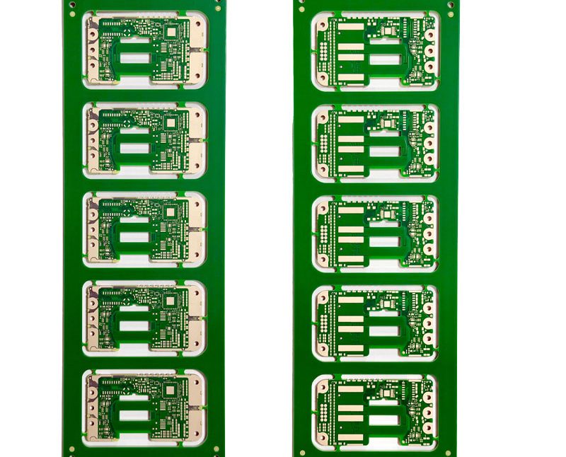
PCB Breakaway Tab Setup: Getting Ready Buyers and engineers often focus on the finished product and forget the production line behind it. In practice, most field failures can be traced back to process decisions made during assembly. Understanding PCB breakaway tab setup gives you a practical advantage when you choose…
PCB Breakaway Tab Defects: What Goes Wrong Electronics manufacturing has become a discipline of small details. Solder paste volumes, placement accuracy, temperature profiles and inspection limits all add up to the final result. This guide looks at PCB breakaway tab defects from the perspective of a PCBA factory floor, covering…