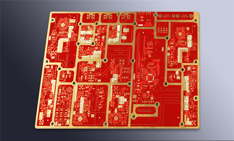
Solder Mask Jetting: Inkjet Printing for Fine Features Solder mask jetting is the deposition of solder mask ink directly onto the board through an inkjet print head, with no screen, no film and no development step. The head writes the pattern from the CAD data, so a change to a…
PCB Statement of Work Sample: Checking a Small Piece Electronics manufacturing has become a discipline of small details. Solder paste volumes, placement accuracy, temperature profiles and inspection limits all add up to the final result. This guide looks at PCB statement of work sample from the perspective of a PCBA…
Etchant Analysis: Keeping Copper Etch Chemistry in Balance Etchant analysis is the routine measurement of the chemistry that dissolves copper, and it exists because the etch rate drifts as copper accumulates and the oxidising power of the bath falls. A bath that is not analysed etches slowly at the start…
Steam Aging for Solderability Testing: 7 Process Rules Steam aging is a preconditioning step rather than a test in itself. It exposes a test coupon to hot, condensing moisture for a defined period so that the surface oxide grows in hours to something like the condition a board would reach…
Laminography: 3D X-Ray Imaging for Solder Joints Laminography, also called computed laminography or tomosynthesis, produces an X-ray image of one plane inside an assembly while the material above and below that plane is blurred out. The result is a view of a single solder joint layer without the superposition that…
Lead Tinning: 6 Rules for Component Solderability Lead tinning is the operation that replaces a component lead finish with fresh solder so that the part can be soldered reliably in a later assembly step. It is common on parts with aged, oxidised or incompatible finishes, and on hardware and connectors…
Tin Pest in PCB Finishes: 6 Rules for Cold Storage and Alloys Tin pest is the transformation of white tin, the familiar ductile metal, into grey tin, a brittle phase that crumbles to powder. The change becomes possible below about thirteen degrees Celsius, it is slow at first and then…
Dye Penetrant Testing for BGA Joint Cracks and Voids Dye penetrant testing is a destructive method in which a coloured fluid is drawn into every crack in a solder joint before the package is separated from the board. When the joint is opened, the stained area is the crack, and…
Trace Repair and Jumper Wires on PCB Assemblies: 7 Rules A trace repair is the last resort before a board is scrapped. A conductor that has been cut by a probe, torn during rework or cracked by repeated flexing can often be restored, but the repair has to carry the…
PCB Statement of Work Risks: What Could Go Wrong Modern electronics depend on boards that are assembled correctly the first time. Every product – a phone, a charger, a medical instrument or an industrial controller – relies on thousands of solder joints that must conduct current for years. This article…