Solder Mask Jetting: Inkjet Printing for Fine Features
Solder mask jetting is the deposition of solder mask ink directly onto the board through an inkjet print head, with no screen, no film and no development step. The head writes the pattern from the CAD data, so a change to a pad opening is a change to a file rather than a change to a tool.
Inkjet printing for solder mask is used for prototype and small volume work where the cost of a screen or a photo tool cannot be justified, and increasingly for production where very small mask openings or unusual geometries are required. Its limits come from the ink and the head rather than from the imaging process.
What Solder Mask Jetting Is
A jetting machine holds one or more print heads above a moving table. Each head fires droplets of mask ink at a controlled rate, and the pattern is built up by raster scanning the head across the panel, so the opening geometry is defined by software rather than by a mask artwork.
Because the deposit is written, the process can vary thickness locally. An area that needs more coverage receives more passes, while a region where a thin coating is sufficient receives fewer. That flexibility is the main reason the process is used where a conventional mask cannot meet the drawing.
Jetting Compared With Photoimageable Mask
A photoimageable mask is applied over the whole panel and then imaged, so the ink that is not wanted is developed away. Jetting applies ink only where it is wanted, which removes the developer step and the associated waste, and it also removes the dimensional change that a photo tool introduces through thermal expansion.
The trade is speed and cost. Jetting is slower per unit area than screen printing, and the ink is more expensive. For a panel with a large masked area and generous features, the conventional route remains cheaper; for a small panel with fine openings, the balance often moves toward jetting.
Ink Chemistry and Viscosity
Jetting ink is formulated with a much lower viscosity and a different flow behaviour than screen ink. It is typically a low viscosity formulation, often in the range of 20 to 50 mPa·s at the jetting temperature, and the head holds it at an elevated temperature, commonly 40 to 60 C, so that it remains stable in the nozzle.
Temperature control is therefore part of the ink specification. A head that runs cool produces satellites and irregular droplets, while one that runs hot dries ink in the nozzle and interrupts the jet. Both symptoms look like a head fault and are in fact a thermal control fault.
Resolution and Feature Limits
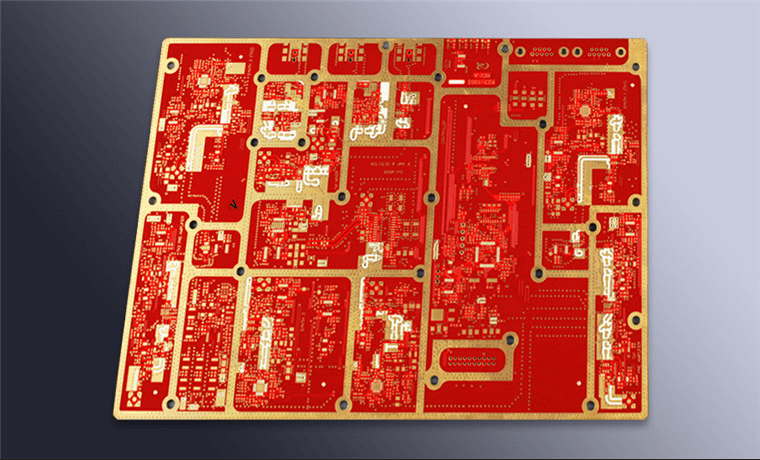
Resolution depends on droplet volume, placement accuracy and ink spread on the surface. Modern heads produce droplets of a few tens of picolitres, which translates into mask features in the 50 to 100 um range, with the smaller figures achievable only on a surface with the right treatment.
Surface energy is the limiting factor. Ink that wets too readily spreads beyond the intended edge, so the opening closes and the pad definition suffers. Ink that does not wet sufficiently beads and leaves a ragged edge. Plasma treatment before jetting is commonly used to place the surface in the middle of that window.
<img src="https://www.gopcba.com/wp-content/uploads/2026/08/hdi-pcb-design-guidelines-11-b6900f71.webp" alt="PCB panel with jetted solder mask openings over fine pitch pads” />
Deposition Thickness and Coverage
Thickness is controlled by the number of passes and the overlap between them. A single pass may deposit 10 to 15 um, and the final thickness on a finished board is usually in the range of 15 to 30 um over the conductor, depending on the ink system and the standard being applied.
Coverage over conductor edges is the property that matters most, because that is where the coating is thinnest and where adhesion is tested. Measuring thickness on a coupon with a step or by a non destructive film gauge gives the number, and the same coupon should be checked after the thermal excursions of assembly. Adhesion should be confirmed on the same specimen using a cross hatch method such as the solder mask adhesion test.
Cure of a Jetted Mask
Jetted ink cures by the same mechanisms as screen printed ink, usually a thermal cure with an optional ultraviolet stage to hold the pattern in place. Because the deposit is thinner and applied without a screen, the cure schedule can differ from the screen printed schedule for the same chemistry family.
Full cure still has to be verified rather than assumed. A jetted coating that is under cured behaves like any other under cured mask, absorbing flux and cleaning chemistry and losing adhesion at the pad edge, and the diagnosis is the same: a measured cure verification result rather than an oven set point.
Keep-Out Areas and Pad Definition
Jetting defines the pad opening precisely because the ink is placed rather than imaged, but the pad still needs a keep-out margin. A mask edge placed too close to the pad can lift during soldering, and one placed too far away leaves exposed copper that can bridge after reflow.
A common working figure is a mask opening 50 to 100 um larger than the copper pad, with the exact value set by the assembly house and the pitch. Because the value is held in software, it should be checked against the drawing rather than assumed to have been transferred correctly.
Process Control and Head Maintenance
The head is the most attention hungry part of the machine. Nozzle plates are cleaned on a schedule, droplet formation is checked visually or with a drop watcher, and a nozzle that has stopped firing is detected by the missing line it leaves rather than by an alarm.
Registration should be verified on every job. Fiducial recognition sets the coordinate frame, and the deviation between the programmed opening and the printed opening is measured on a sample board. A drift of more than about 25 um on fine pitch work is a reason to stop and recalibrate rather than to adjust the file.
Where Jetting Fits in Production
Jetting suits quick turn work, panels with a small number of fine openings, and products where the mask geometry changes often. It also suits situations where the print quality of a conventional screen process is limited by the screen itself.
It is a poor fit for a large, simple panel produced in volume, where the deposition rate is the deciding cost. The rational approach is to compare the two routes on the actual panel, including the cost of tooling, and to choose on that comparison rather than on the technology alone. The same judgement applies to inkjet legend printing, which shares the head technology and much of the same economics.
FAQ
What is solder mask jetting? It is an inkjet process that writes solder mask ink directly onto the board in the required pattern, removing the screen printing and development steps used by conventional mask processes.
Does jetted solder mask need curing? Yes. The ink is cured thermally, sometimes with an ultraviolet stage first, and the cure state should be verified with the same tests used for any other mask system.
Can jetted mask replace screen printing for volume production? For large, simple panels the deposition rate usually favours screen printing. Jetting wins where features are fine, geometry changes frequently, or the tooling cost of a screen cannot be recovered.
}