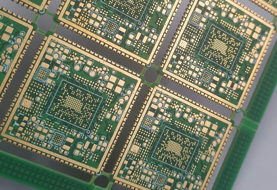
Copper Filled Via Reliability in Multilayer Boards A filled via is a plated hole that has been plugged with a conductive or non conductive material so that the surface can be used as a pad. The technique is what makes via in pad possible, and it is used on every…
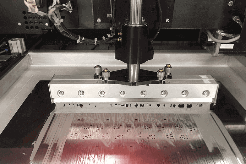
Paste Volume and Print Verification Paste volume is the single largest influence on solder joint quality, and it is also the variable that a production line can measure most easily. Every joint on the board begins as a printed deposit whose height, area and shape decide how much solder will…
Reflow Profile Development and Control A reflow profile is the temperature history the assembly experiences as it passes through the oven, and it decides whether the solder forms a sound joint or merely melts. Building one is an exercise in satisfying several constraints at once: the alloy needs to reach…
Assembly Process Capability and Control Charts A capability index compares the spread of a process with the tolerance it has to meet. A control chart shows whether the process has moved. The two answer different questions and both are needed. What Capability Answers The index compares the process spread with…
BGA Solder Ball Alloy Selection A ball grid array package carries its own spheres, pre attached by the component supplier, and the assembly process joins those spheres to pads with paste. The alloy of the ball and the alloy of the paste are therefore two separate choices that meet at…
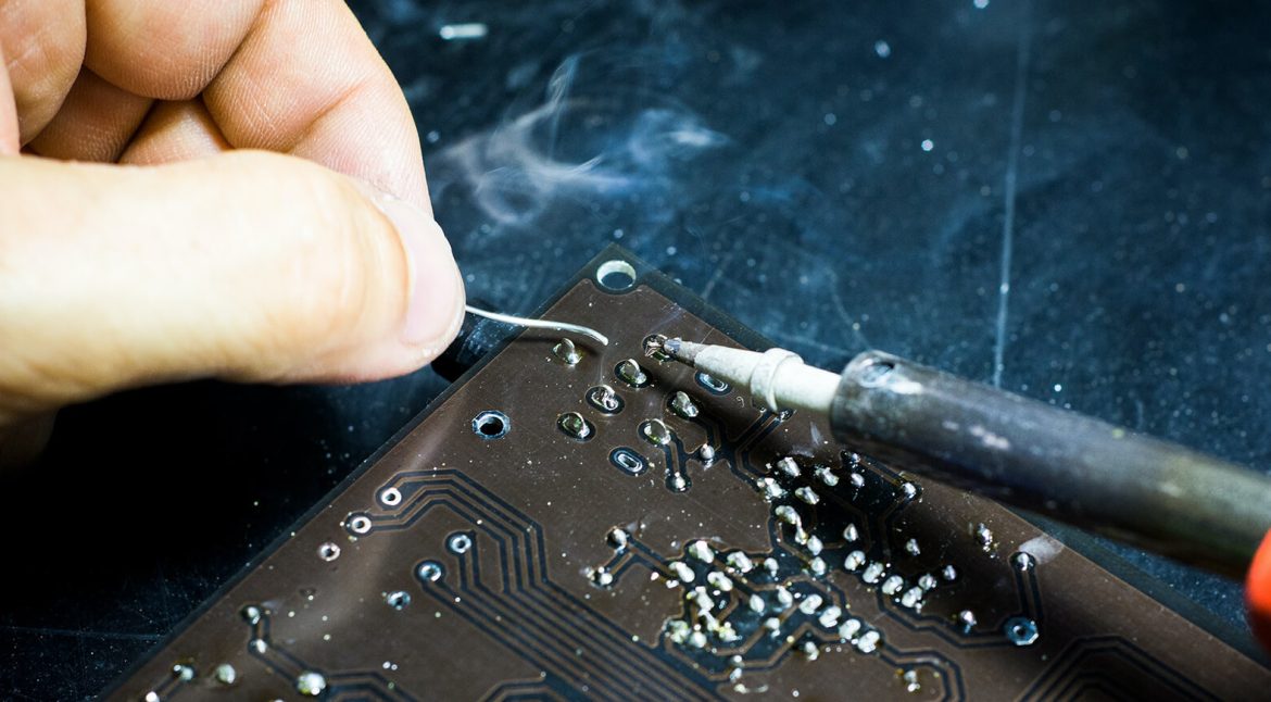
Desoldering and Rework Techniques Compared Every assembly eventually needs a joint remade. Removing solder is a different problem from adding it, because the joint has to be heated through a board that may already be populated, and the surrounding material has seen at least one thermal cycle. The methods differ…
PCB Traceability Audit: Checking the Practice Buyers and engineers often focus on the finished product and forget the production line behind it. In practice, most field failures can be traced back to process decisions made during assembly. Understanding PCB traceability audit gives you a practical advantage when you choose a…
PCB Traceability Problems: When It Goes Wrong Electronics manufacturing has become a discipline of small details. Solder paste volumes, placement accuracy, temperature profiles and inspection limits all add up to the final result. This guide looks at PCB traceability problems from the perspective of a PCBA factory floor, covering troubleshooting…
Controlled Impedance: Preparation, Placement and Process Control Controlled impedance turns a geometric feature into an electrical specification. A trace of a given width, on a given layer, above a given reference plane has a characteristic impedance, and the design says that impedance must stay within a tolerance. Making that true…
Solder Mask Thickness and Its Effect on Assembly Solder mask is drawn as a two dimensional pattern, but it is printed as a three dimensional layer. Its thickness decides whether the mask can cover a tall trace, whether a dam between two pads survives assembly and whether a via is…