Copper Filled Via Reliability in Multilayer Boards
A filled via is a plated hole that has been plugged with a conductive or non conductive material so that the surface can be used as a pad. The technique is what makes via in pad possible, and it is used on every dense board that places a component directly over a via. The requirement is not simply that the hole is filled, but that the fill survives lamination, plating and reflow without shrinking, cracking or contaminating the plating bath. A filled via is therefore a materials problem as much as a process problem, and the material has to be chosen for the sequence it will experience.
Why Vias Are Filled
An open via cannot be used as a pad, because the paste printed over it drains into the barrel during reflow and leaves an incomplete joint. Filling the via removes the void and gives the paste something to sit on, which is what allows a via in pad design.
Filling is also used to prevent wicking of flux and coating into the hole, to stop solder from flowing through to the other side, and to provide a flat surface for a fine pitch component. Each application has a slightly different requirement for planarity and for conductivity. The requirement should be written into the fabrication drawing, because a plug that suits one application may fail another.
Filling Materials
Epoxy based plugs are the most common, usually filled with a ceramic or a metal powder to control the thermal expansion and the conductivity. Conductive pastes containing silver or copper are used where an electrical connection through the fill is required.
The material has to survive the process it will see. A plug that is applied before lamination has to withstand the press temperature, while one applied after plating only has to survive the assembly reflow. The choice follows the sequence rather than the other way round. A material that is selected for its conductivity and not for its thermal stability will be the wrong choice on a board that is laminated after filling.
The Filling Process
The material is applied by screen printing or by a dedicated via filling machine, and the hole has to be filled from one side without leaving a void in the middle. Filling is often done in two passes, with a partial cure between them, to avoid trapping air in the barrel.
Excess material is squeegeed off the surface, but a controlled amount is usually left so that the fill compensates for the shrinkage that occurs during cure. Getting that allowance right is one of the practical skills of the process. A machine that dispenses a fixed volume works well where the via geometry is constant, and less well where the panel carries several different hole sizes.
<img src="https://www.gopcba.com/wp-content/uploads/2024/09/5.jpg" alt="Via fill material being screen printed into a PCB panel” />
Dishing and Planarity
Dishing is the recess that forms at the top of the fill as the material shrinks during cure. A small recess is acceptable in some applications and not in others, and the acceptance limit should be stated as a number rather than as an impression. Planarity is normally measured by comparing the fill surface with the surrounding copper on a microsection or with an optical profilometer.
Planarity matters most for a via in pad, because a recess under a paste deposit changes the volume of paste that the joint receives. Our hole copper guide explains how the barrel and the fill interact in the finished hole. Where the recess is measured on a coupon and found to be outside the limit, the fill volume or the cure profile is the usual culprit.
Plating Over the Fill
Where the filled via will be plated and used as a pad, the fill has to be compatible with the plating chemistry. A plug that outgasses or that leaches into the bath contaminates the solution and can affect every panel in the load. Filtering the plating bath and monitoring the organic content is the usual defence on a line that plates over filled vias.
The plating also has to adhere to the fill. A cap that sits on the plug rather than on the surrounding copper can lift during thermal cycling, so the design usually includes an annular ring of copper for the plating to bond to. Our plating thickness guide covers the measurement of the cap. The cap thickness over a filled via is normally measured on a section, because the X-ray method cannot separate the cap from the surrounding copper.
Reliability Under Thermal Cycling
The plug, the copper barrel and the surrounding laminate expand at different rates, so thermal cycling loads the interface between them. A plug with a thermal expansion coefficient far from that of the laminate will pump the barrel and eventually cause a crack.
The risk is highest where the via is large, where the wall is thin, or where the assembly sees a wide temperature range. Where the application is demanding, the fill and the barrel geometry should be qualified together rather than separately. A cycling test on a coupon with the production fill is the practical way to qualify the combination for a demanding application.
Defects and Detection
The common defects are an incomplete fill with a void in the middle, a crack between the fill and the barrel, dishing beyond the limit and delamination around the via after thermal stress. None of them is reliably visible from the surface. A via that looks flat and well filled can still contain a void that will open during the first thermal cycle.
Detection is by microsection after a thermal stress, and by X-ray where the fill is dense enough to show a contrast. Our quality documentation describes how these conditions are classified at gopcb.
Design Rules for Filled Vias
The design has to give the process room. The via diameter should be within the range that the filling equipment can handle reliably, the annular ring should be wide enough for the plating cap, and the material should be specified rather than left to the fabricator. Where the material is critical to a thermal requirement, specifying the conductivity as well as the fill material prevents a surprise.
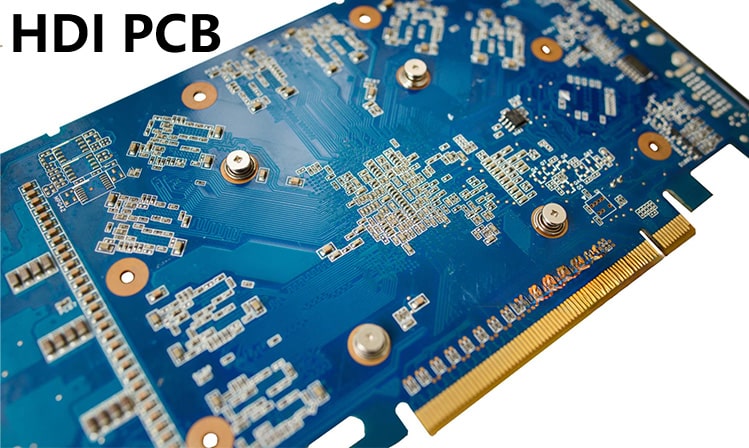
Where the via is inside a thermal pad, the fill also has to conduct heat. Our HDI guide covers the via structures and the process sequences that dense boards use. Blind and buried vias are often filled for the same reasons, with the additional constraint of the lamination sequence.
Process Control Points
The controls are the material lot and its shelf life, the mixing and the working life, the fill method and the number of passes, the cure profile, the planarity measurement, the plating compatibility and the results of the thermal stress test.
Because the fill is hidden once the board is finished, prevention depends on the process record. A coupon that follows the panels through the fill, the cure and the plating is the evidence that the production vias received the same treatment. Without that coupon a failing lot cannot be distinguished from a good one until the boards reach the field.
FAQ
Does a filled via have to be conductive? Not always. A non conductive plug is fine where the via only has to be flat, while a conductive fill is needed where the plug forms part of the electrical or thermal path.
What is dishing and how much is acceptable? Dishing is the recess at the top of the plug caused by shrinkage during cure. The acceptable amount depends on the application and should be stated as a measured limit.
Why does a filled via crack after thermal cycling? Because the plug, the copper and the laminate expand at different rates. Matching the fill to the application and testing it on a coupon is what prevents the failure.