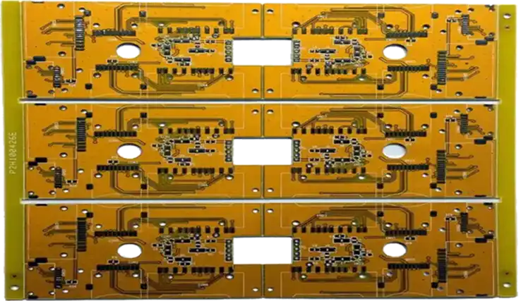
Panelization and Depaneling: Design Rules and Cost Panelization is the arrangement that lets an assembly line handle a small board, and depaneling is the step that returns it to a single unit. Both are decided at layout, and both cost money if the arrangement is chosen after the artwork is…

Copper Thickness Selection for Power and Ground Planes A power plane is usually specified by its finished copper weight rather than by a dimension, and the two are related but not identical. The figure on the drawing sets the current the plane can carry, and it also sets what the…
Via in Pad: Filling, Planarization and Assembly Rules Via in pad places the via inside the solder pad so the ball or the printed paste lands on the same feature that carries the signal to the next layer. The arrangement saves routing space on dense boards, but it moves a…
Thermal Interface Degradation Over Product Life A thermal interface is specified by its resistance when new and by its stability over the life of the product. The second number is the one that decides whether the design still works after a year. Pump Out and Dry Out A grease migrates…
Visual Inspection Criteria for Lead Free Solder Joints Lead free solder looks different from tin lead. It is more matte, it does not always form a smooth concave fillet and its surface is often grainy. Criteria written for the older alloy reject joints that are perfectly sound. Why the Appearance…
Reflow Assembly of Flexible and Rigid Flex Circuits A flexible circuit is thin, it moves and it is soldered in the same process as a rigid board. Each of those properties changes how the reflow has to be controlled. Why Flex Behaves Differently The material is thin, so it heats…
QFN and Bottom Termination Component Soldering A quad flat no lead package sits on its pads rather than on leads, so the joint is formed at the edge of the package and it is short. The joint that forms is often thinner than the design assumed. Why the Joint Is…
Barrel Crack: Plated Through Hole Reliability Under Thermal Cycling A plated through hole is a copper tube in a laminate that expands more than the copper does. Every thermal cycle loads the barrel at its two ends, and the crack that forms is the classic board level failure. The Load…
PCB Labeling Setup: Getting Ready Electronics manufacturing has become a discipline of small details. Solder paste volumes, placement accuracy, temperature profiles and inspection limits all add up to the final result. This guide looks at PCB labeling setup from the perspective of a PCBA factory floor, covering setting up labeling…
PCB Labeling Training: Teaching the Team Modern electronics depend on boards that are assembled correctly the first time. Every product – a phone, a charger, a medical instrument or an industrial controller – relies on thousands of solder joints that must conduct current for years. This article explains PCB labeling…