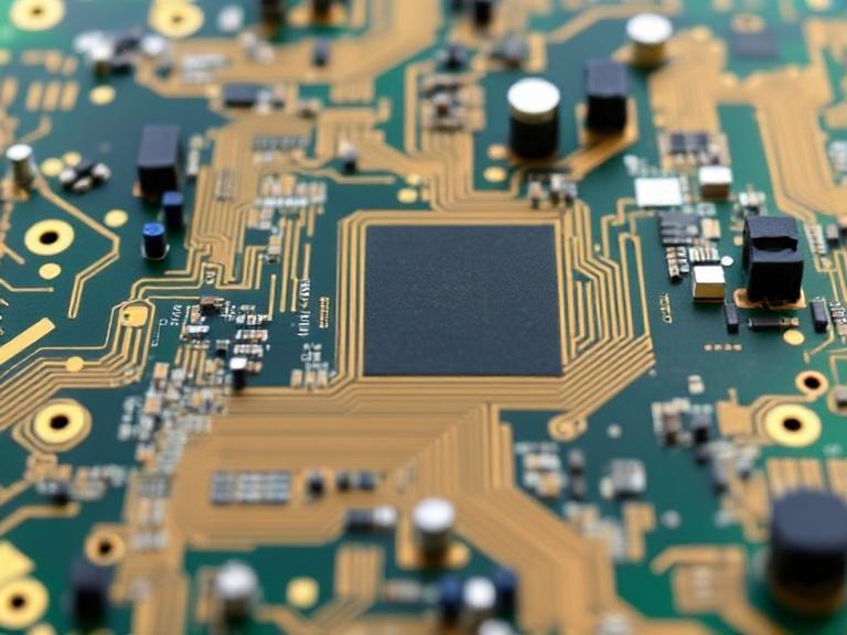
Blind and Buried Via Design Rules: An HDI Stack-Up Guide Blind and buried vias are the reason a dense board can be routed at all. They let a signal travel between two inner layers without drilling through the whole panel, freeing the surface for components and shortening the return path…
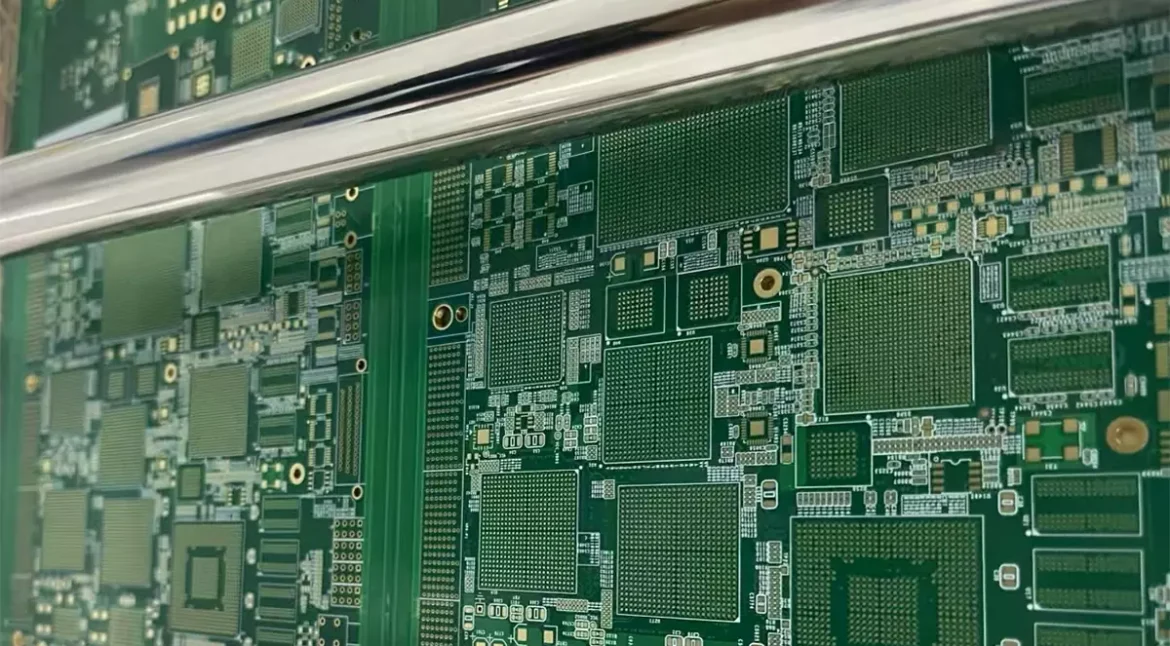
Autorouting High Speed Digital PCBs: Why It Falls Short Autorouters have improved enormously, and for many boards they are genuinely useful. Yet on a high speed digital design they still produce results that experienced engineers reject, and the reason is not that the algorithms are weak. It is that the…
Two-Layer Board: Two-Layer vs Four-Layer PCB: What the Extra Layers Buy The number of copper layers is the single choice that most affects the cost of a board, and it is usually made early, on the strength of an estimate rather than a calculation. Understanding what the second and third…
Solder Wicking and Thermal Relief Design in PCB Layout Two solder problems that look unrelated share the same root cause. Solder wicking pulls molten alloy where it does not belong, and thermal relief design decides how heat moves between a pad and the plane it touches. Both are controlled by…
Automotive PCB Price Guide: ECU, ADAS and Body Control An automotive control board is specified for a lifetime and an environment rather than for a function, and that is what makes its price structure different from any consumer board. A four-layer board with the same circuit can cost three times…
Through-Hole vs Surface Mount Assembly: Choosing the Process The choice between through-hole and surface mount assembly is usually settled by the component list rather than by the board, but the consequences reach back into the layout. Where both technologies appear on one board, the order in which they are assembled…
PCB Stack-Up Design for EMI Reduction: A Practical Guide Stack-up decisions are made early, before layout starts, and they set a ceiling on how quiet the finished board can be. A stack-up that places every signal layer next to a solid reference plane and keeps the layer-to-plane spacing small behaves…
Solder Paste Storage and Handling: A Process Guide Solder paste is a mixture of metal powder and flux that begins to change the moment it is opened, and most printing defects that are blamed on the stencil can be traced back to how the paste was stored, thawed and handled…
PCB Lead Free Transition: Leaving the Lead Behind Modern electronics depend on boards that are assembled correctly the first time. Every product – a phone, a charger, a medical instrument or an industrial controller – relies on thousands of solder joints that must conduct current for years. This article explains…
PCB Serialization and Traceability: Naming Every Board Modern electronics depend on boards that are assembled correctly the first time. Every product – a phone, a charger, a medical instrument or an industrial controller – relies on thousands of solder joints that must conduct current for years. This article explains PCB…