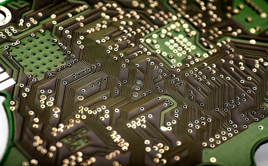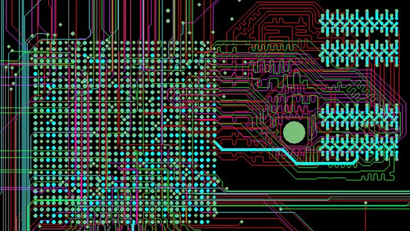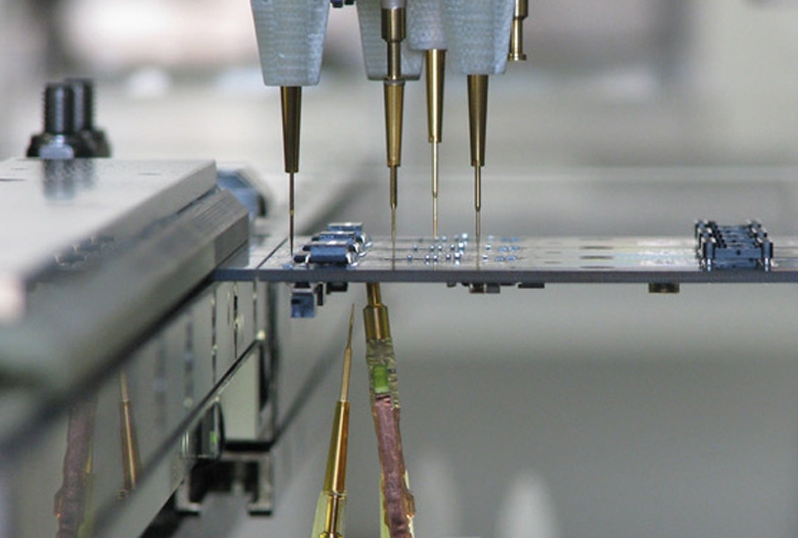
Copper Pour on Outer Layers: When It Helps and When It Hurts Pouring copper over the empty area of an outer layer is one of those steps that is usually recommended and rarely explained. Done well it improves shielding, spreads heat and helps the board survive reflow. Done badly it…
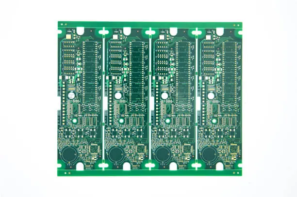
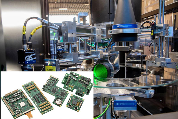
PCB Audio Ground Noise: Chasing the Hum Buyers and engineers often focus on the finished product and forget the production line behind it. In practice, most field failures can be traced back to process decisions made during assembly. Understanding PCB audio ground noise gives you a practical advantage when you…
PCB Matching for An Antenna: The Parts Between Them Modern electronics depend on boards that are assembled correctly the first time. Every product – a phone, a charger, a medical instrument or an industrial controller – relies on thousands of solder joints that must conduct current for years. This article…
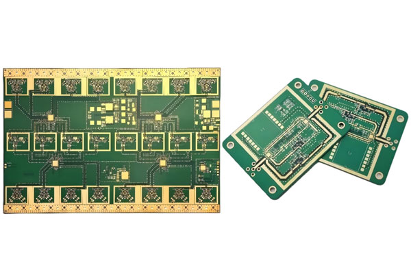
Hybrid Stackup Design: Mixing High Frequency and FR4 An all high frequency board solves every electrical problem and creates a cost problem, because the material alone can be many times the price of an ordinary laminate. A hybrid stackup takes the opposite approach: it uses the expensive dielectric only where…
Capacitor Polarity on a PCB: Markings, Mistakes and Consequences Reversing a polarized capacitor is one of the rare assembly errors that damages the board as well as the component, and it is also one of the easiest to prevent. The marking conventions are consistent once they are understood, and the…
PCB Antenna Tuning: Matching the Length Buyers and engineers often focus on the finished product and forget the production line behind it. In practice, most field failures can be traced back to process decisions made during assembly. Understanding PCB antenna tuning gives you a practical advantage when you choose a…
PCB Design File Checks Before You Order Most delays on a prototype order come from questions the fabricator has to ask before the data can be processed. The board is quoted from the design files once they are converted into production data, and the fabricator never sees the schematic, so…
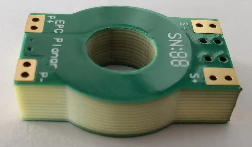
Any Layer HDI PCB: Stackups, Microvias and Build Sequence Any layer HDI removes a constraint that older high density designs accepted as a rule. In a conventional HDI stack the microvias connect only the outer layers to the next one, so a signal that has to reach an inner layer…
PCB Thermal Deformation: Tg, CTE and Z-Axis Expansion A circuit board changes shape when it is heated, and the change is not uniform. The laminate expands more in the thickness direction than in the plane, the copper expands less than the resin, and above a certain temperature the resin softens…
PCB RF Antenna Keepout: Space Around the Antenna Modern electronics depend on boards that are assembled correctly the first time. Every product – a phone, a charger, a medical instrument or an industrial controller – relies on thousands of solder joints that must conduct current for years. This article explains…