PCB Wick and Braid for Desoldering: Taking the Solder Away Buyers and engineers often focus on the finished product and forget the production line behind it. In practice, most field failures can be traced back to process decisions made during assembly. Understanding PCB wick and braid for desoldering gives you…

Electroless Copper vs Electroplated Copper in PCB Fabrication Two very different copper processes share a similar name in most discussions of board fabrication, and confusing them leads to wrong expectations about thickness and reliability. Electroless copper deposits a very thin conductive layer by chemical reduction, and electroplated copper builds the…
ESD Protection in PCB Layout: Techniques That Work Electrostatic discharge is one of the few design problems that never announces itself. A board that fails an ESD test is easy to deal with; a board that passes every bench measurement and then resets once a week in the field is…
PCB Solder Preform for A Shield: Sealing the Frame All Round Buyers and engineers often focus on the finished product and forget the production line behind it. In practice, most field failures can be traced back to process decisions made during assembly. Understanding PCB solder preform for a shield gives…
PCB Pin Soldering By Hand: Iron Meets Pin Electronics manufacturing has become a discipline of small details. Solder paste volumes, placement accuracy, temperature profiles and inspection limits all add up to the final result. This guide looks at PCB pin soldering by hand from the perspective of a PCBA factory…
PCB Solder Preform Placement: A Piece of Solder in Place Buyers and engineers often focus on the finished product and forget the production line behind it. In practice, most field failures can be traced back to process decisions made during assembly. Understanding PCB solder preform placement gives you a practical…
Press-Fit Holes in PCBs: Tolerances, Pin Types and Reliability A press-fit joint makes an electrical connection by forcing a compliant pin into a plated hole, without solder. The pin deforms elastically as it enters, the hole is slightly smaller than the pin, and the resulting contact pressure holds the two…
PCB Stencil Aperture for A Connector Pad: Enough Paste for a Big Pad Electronics manufacturing has become a discipline of small details. Solder paste volumes, placement accuracy, temperature profiles and inspection limits all add up to the final result. This guide looks at PCB stencil aperture for a connector pad…
Aluminum PCB or FR4: Choosing by Heat and Cost A metal backed board and a conventional FR4 board are often compared as if one were simply a better version of the other. They are not: they solve different problems, and the aluminium choice is justified by heat or by mechanical…
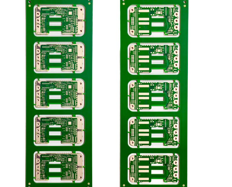
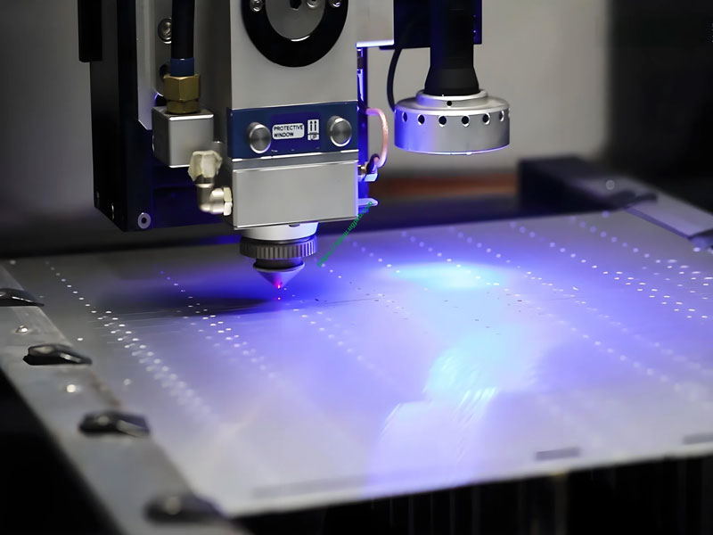
PCB Routing Precision: Outline Tolerance and Edge Quality Routing is the operation that gives a printed circuit board its final shape. A CNC cutter follows the outline, cuts slots and windows and separates the individual circuits from the production panel, and the accuracy of that operation decides whether the board…