Copper Balance and Warpage in Multilayer PCB Lamination
Warpage in a multilayer board is usually blamed on the press, and the press is often innocent. The board warps because the stresses built into it during lamination are unbalanced, and the most common source of imbalance is the distribution of copper. Understanding how the laminate is built explains why an apparently harmless decision about a plane or a pour changes how flat the finished board is.
How a Multilayer Board Is Built
A multilayer board is assembled from cores and prepreg. A core is a sheet of laminate with copper foil bonded to both faces and etched into a pattern. Prepreg is a partially cured resin-impregnated glass cloth that acts as the adhesive between cores. The stack is pressed under heat and pressure, the resin flows and then cures, and the result is a single rigid board with the copper layers embedded in it.
During the press the resin shrinks as it cures, and the copper constrains that shrinkage. Where there is a lot of copper, the resin is held back; where there is little, it shrinks freely. If the two halves of the stack-up are not symmetrical in this respect, the finished board will bow when it cools, because one side contracts more than the other.
What Copper Balance Means
Copper balance is the requirement that the amount and the distribution of copper be approximately equal on either side of the stack-up’s centre line. A board with a solid ground plane on one inner layer and an almost empty signal layer directly opposite is unbalanced, however good the layer assignment looks on paper.
In practice, balance is achieved by combining three measures: keeping the placement of large copper areas symmetrical between the two halves of the stack-up, filling empty regions with a pour or a cross-hatched pattern so that the local copper density is more uniform, and avoiding large copper areas that exist on one side only. A signal layer with sparse routing opposite a solid plane is a common cause of a board that curves after assembly.

Thickness and the Limits of Availability
Stack-up design is constrained by what the material supplier offers. FR-4 is available in a wide range of thicknesses, which is one reason it remains the default for multilayer boards. Specialised materials come in fewer options: a high-frequency laminate may be produced in only a handful of standard thicknesses, and the choice of an unfamiliar material can limit the stack-up before any electrical consideration is reached.
A designer who needs a specific dielectric separation for a controlled impedance has to find a combination of cores and prepreg sheets that delivers it. Where the material’s available thicknesses do not allow the required separation, the options are to change the material, change the impedance target or accept an additional layer to reach the required geometry.
Material Properties That Matter
Two material parameters influence the design most: the dielectric constant and the loss factor. The dielectric constant sets the trace geometry needed for a given impedance and the propagation velocity of the signal. The loss factor determines how much of the signal energy is absorbed by the laminate, which becomes significant as the frequency rises.
The dielectric constant of FR-4 varies between manufacturers and between batches, commonly in the range from about 4.2 to 5.4. For a board operating below a gigahertz this variation is usually tolerable, and the mature lamination process keeps the cost low. Above that, the variation starts to matter, and a material with a more tightly specified dielectric constant becomes the safer choice.

Choosing a Material by Frequency
Below about one gigahertz, FR-4 covers most requirements. Where the impedance is low, such as a fifty-ohm line, the characteristic impedance and the coupling between adjacent traces still have to be controlled carefully, and the variation between FR-4 batches should be accounted for in the tolerance budget.
For optical communication products operating above roughly 622 megabits per second, and for small-signal microwave transceivers between one and three gigahertz, a modified epoxy material offers a more stable dielectric constant at a modest cost premium, and it can be processed on the same multilayer lamination line as FR-4. Above three gigahertz, laminates in the polytetrafluoroethylene family become the practical choice, and above ten gigahertz they are effectively required. Our high-frequency laminate notes cover the material families in more detail, and the PTFE material page describes the processing differences.
Designing Within the Process
The practical conclusion is that stack-up design begins with the material data sheet rather than with the impedance calculation. Establish what thicknesses and what copper weights the chosen laminate is available in, confirm that the laminates are symmetric about the centre line, and check the copper distribution on each layer before the artwork is generated. A stack-up that satisfies the electrical requirement but not the balance requirement will produce boards that are electrically correct and mechanically out of specification.
The layer count selection notes explain how the stack-up is planned, the laminate material properties page covers the parameters that drive the choice, and the design release checklist includes the checks that should be applied before the stack-up is frozen.
Detecting an Unbalanced Design Before the Press
Balance problems are cheap to find on the artwork and expensive to find in the press. The check is to compare, for each layer, the proportion of the panel covered by copper, and to compare the two halves of the stack-up rather than the two outer layers. A layer that is mostly copper opposite a layer that is mostly empty is the pattern to look for, whatever the total copper on the board. Where the imbalance is large, a cross-hatched fill on the empty layer reduces it without changing the electrical behaviour appreciably.
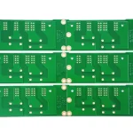
It is also worth checking the copper balance across the panel rather than within a single board. A panel with a dense rail of boards on one side and sparse boards on the other will warp even if each board is balanced on its own, because the press sees the panel. Coupons, borders and tooling strips all contribute copper to that balance and should be counted in the assessment.
FAQ
How much warpage is acceptable? The usual specification for a rigid board is expressed as a maximum bow and twist measured against the board diagonal, and the figure is commonly a fraction of a percent, with a stricter value applied to boards intended for automated assembly. The requirement should be stated with the order, because a board that is acceptable for a hand-assembled product may not be acceptable on a placement machine.
Does a heavier copper weight make warpage worse? It can, because thicker copper constrains the resin more strongly and therefore increases the differential stress if the copper distribution is unbalanced. Heavier copper also requires wider minimum features, which changes the etching process. The remedy is the same in either case: balance the copper distribution and keep the stack-up symmetrical.
What does gopcb review before lamination? We check the stack-up for symmetry, the copper distribution on each layer, and the availability of the specified material thicknesses. Where a design is unbalanced, we raise it before the panels are released, because correcting the balance afterwards means re-engineering the stack-up rather than adjusting a setting.