Capacitive PCB: PCB Design, PCB Manufacturing, Applications & Benefits
A Capacitive PCB is a specialized printed circuit board that uses copper electrodes to detect changes in capacitance caused by the presence or touch of a conductive object, such as a human finger. Unlike mechanical buttons that rely on moving components, capacitive sensor technology provides a durable, responsive, and intuitive interface.
In modern PCB Design and electronic engineering, Capacitive Sensor PCB technology has become an important solution for creating fast and intuitive human-machine interfaces (HMI). By integrating sensing electrodes directly into the PCB layout, engineers can develop compact touch interfaces for consumer electronics, automotive systems, medical equipment, industrial controls, and smart-home devices.
This article explains what a capacitive PCB is, how it works, the materials and design considerations involved, its manufacturing process, applications, advantages, limitations, and cost factors.
What Is a Capacitive PCB?
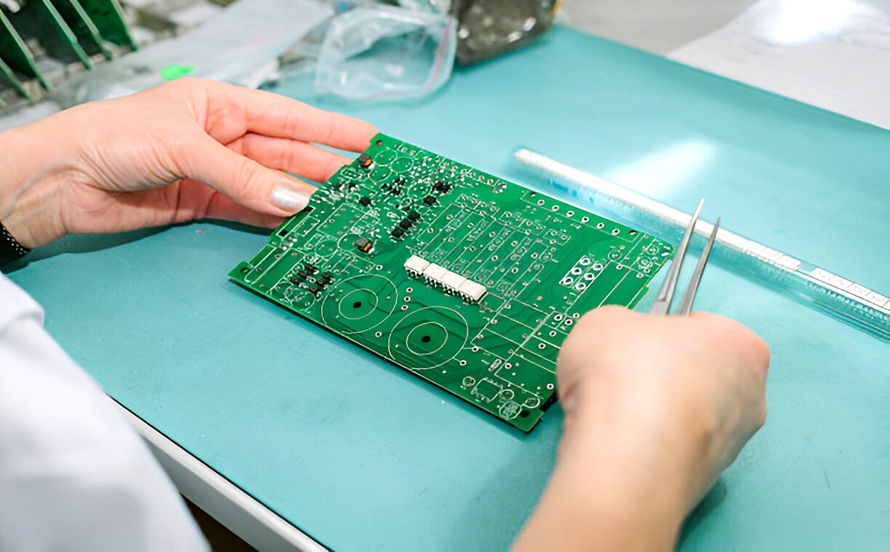
A Capacitive PCB, also called a Capacitive Sensor PCB, is a printed circuit board that detects touch or proximity by measuring changes in capacitance.
The sensing structure generally consists of copper electrodes, dielectric materials, a protective overlay, and a controller or sensing IC. Rather than relying on a discrete capacitor to store electrical energy, the PCB’s copper traces, pads, and planes are intentionally designed to create an electric sensing field.
When a conductive object such as a human finger approaches the sensing electrode, it changes the local electric field and therefore alters the measured capacitance. The controller detects this change and interprets it as a touch, proximity, or gesture event.
This approach allows the PCB itself to function as part of the sensing system, reducing the need for conventional mechanical switches and enabling thinner, more flexible, and more visually integrated interfaces.
Key Characteristics of Capacitive PCBs
A capacitive sensor PCB must be carefully engineered because its electrical performance depends on both the PCB structure and the surrounding environment. Important characteristics include dielectric properties, insulation resistance, parasitic capacitance, dimensional stability, and surface flatness.
1. Dielectric Constant
The dielectric constant of the PCB substrate and protective overlay strongly affects the electric field generated around the sensing electrode.
A stable dielectric constant helps maintain consistent touch sensitivity across the PCB. FR-4 is commonly used for general-purpose designs, while specialized applications may use ceramic, PTFE-based, or other high-performance materials when tighter electrical stability or environmental performance is required.
The dielectric properties of the overlay are also important because glass, acrylic, polycarbonate, and other materials can change the distance and electrical coupling between the user’s finger and the sensing electrode.
2. High Surface Resistivity
The surface surrounding the sensing electrode should provide adequate electrical insulation.
High surface resistivity helps minimize leakage currents and reduces the possibility of unintended triggering. The protective layer, solder mask, and other dielectric materials must therefore be selected and controlled carefully.
3. Low Parasitic Capacitance
Controlling parasitic capacitance is one of the most important challenges in Capacitive PCB Design.
Unwanted capacitance can occur between sensor traces, ground planes, adjacent conductors, and other PCB structures. Excessive parasitic capacitance can reduce the signal-to-noise ratio and make touch detection less reliable.
Designers may optimize trace geometry, increase the distance between sensing traces and ground structures, and carefully control copper geometry to minimize unwanted coupling.
4. Dimensional Stability
Dimensional stability is critical because capacitance is affected by electrode area and the distance between conductive structures.
Changes in PCB dimensions caused by temperature, moisture, or manufacturing variation can therefore affect sensor performance. Stable substrate materials and controlled manufacturing processes help maintain consistent sensing characteristics.
5. Surface Flatness
A capacitive sensor PCB normally works beneath a protective layer such as glass, acrylic, or polycarbonate. A flat and uniform interface helps maintain consistent electrical coupling across the sensing area.
Surface finishes such as ENIG can provide a relatively flat copper surface compared with some conventional finishes. The thickness and uniformity of the solder mask or other dielectric layer should also be controlled because variations can affect the electrical distance between the sensor electrode and the user.
Types of Capacitive PCBs
Different capacitive sensing architectures are used depending on the required touch functionality, form factor, and application.
1. Surface-Capacitive PCB
A surface-capacitive system typically uses a conductive sensing layer connected to a controller. It can provide reliable touch detection but generally has more limited multi-touch capability than projected-capacitive technology.
This architecture is often used when simple touch detection is sufficient.
2. Projected-Capacitive PCB (PCAP)
Projected-capacitive technology, commonly known as PCAP, is widely used in modern touchscreens.
It uses a structured electrode arrangement, often consisting of transmitting and receiving electrodes arranged in rows and columns. The controller monitors changes in mutual capacitance to identify touch locations.
PCAP technology supports accurate touch detection, multi-touch operation, and high sensitivity, making it suitable for smartphones, tablets, automotive displays, industrial HMIs, and other advanced interfaces.
3. Flexible Capacitive PCB
A flexible capacitive sensor circuit can be manufactured on a polyimide substrate.
Because the flexible substrate can bend or conform to curved surfaces, flexible capacitive PCBs are useful in wearable electronics, curved interfaces, automotive interiors, and space-constrained products.
Materials Used in Capacitive PCB Manufacturing
Material selection directly affects the sensitivity, stability, durability, and manufacturing cost of a capacitive PCB.
Common Substrate Materials
Common materials include:
- FR-4 for general-purpose capacitive PCBs
- Polyimide for flexible capacitive circuits
- Glass-reinforced epoxy materials for applications requiring dimensional stability
- Specialized high-performance materials for demanding electrical or environmental conditions
Dielectric Properties
The dielectric properties of the substrate and protective overlay influence:
- Touch sensitivity
- Signal-to-noise ratio
- Electric-field distribution
- Touch detection through protective materials
- Environmental stability
For this reason, the dielectric constant and thickness of the materials should be considered together during PCB Design.
Protective Overlays and Coatings
Depending on the application, the sensing area may be covered with:
- PET film
- Polycarbonate
- Acrylic or PMMA
- Glass
- Controlled solder-mask layers
The thickness, dielectric constant, mechanical strength, and surface properties of the protective material all affect the final sensing performance.
Copper Thickness and Surface Finish
1 oz copper is a common starting point for many PCB applications, although the appropriate copper thickness depends on the electrical and mechanical requirements.
ENIG may be selected where a relatively flat and stable electrode surface is required. In some applications, copper geometry and thickness can also be optimized to control parasitic capacitance.
How Does a Capacitive PCB Work?
The operating principle of a Capacitive Sensor PCB is based on changes in capacitance and electric-field distribution.
A capacitive sensor generally consists of one or more conductive electrodes connected to a sensing controller. When a conductive object approaches or touches the sensing area, it changes the electrical characteristics of the sensor.
Two fundamental sensing methods are commonly used.
Self-Capacitance
Self-capacitance measures the capacitance between an individual sensing electrode and electrical ground.
When a person’s finger approaches the electrode, the finger introduces additional capacitive coupling to ground. The resulting capacitance change can be detected by the controller.
Self-capacitance can provide high sensitivity and is relatively straightforward for simple touch or proximity detection. However, multiple simultaneous touches can create ambiguity in some electrode configurations.
Mutual Capacitance
Mutual-capacitance sensing measures the coupling between two electrodes, generally referred to as transmitting and receiving electrodes.
A touch changes the electric field between these electrodes, producing a measurable change in mutual capacitance. By scanning multiple electrode intersections, a controller can determine the location of one or more touches.
This approach is widely used in projected-capacitive touch interfaces.
Signal Processing
Capacitive sensing does not end with detecting a capacitance change. The controller may also perform:
- Noise filtering
- Baseline tracking
- Drift compensation
- Environmental compensation
- Humidity compensation
- Temperature compensation
- Touch threshold adjustment
These functions help maintain reliable performance under changing environmental conditions.
Capacitive PCB Design Considerations
Compared with conventional digital PCB layouts, capacitive sensing circuits require more careful control of the physical geometry and electrical environment.
Sensor Trace Geometry
The shape and size of the sensing electrode have a direct influence on sensitivity.
Common electrode geometries include:
- Circular electrodes
- Diamond-shaped electrodes
- Rectangular electrodes
- Finger-shaped or interdigitated structures
The electrode should be designed according to the required touch area, overlay thickness, sensing method, and controller specifications.
Ground Plane Placement
A ground plane can help control electromagnetic interference (EMI), but placing grounded copper too close to a sensing electrode may reduce sensitivity by increasing parasitic capacitance.
Therefore, the distance between the sensor and surrounding ground structures should be carefully controlled.
Protective Overlay
The thickness and dielectric constant of the glass, plastic, acrylic, or other protective overlay determine how strongly a finger couples to the sensor.
A thicker overlay generally reduces capacitive coupling and may require a larger sensing electrode or a more sensitive controller.
Routing and Noise Control
Sensor traces should be routed away from high-speed digital signals, switching power supplies, clocks, and other major noise sources whenever possible.
Guard structures, shielding techniques, filtering, and appropriate grounding can be used when necessary.
Environmental Considerations
Temperature, humidity, water, contamination, and nearby conductive materials can affect capacitance measurements.
For applications exposed to moisture or chemicals, the sensor structure and protective layer should therefore be designed as part of the complete system rather than treating the PCB independently.
Capacitive PCB Manufacturing Process
The Capacitive PCB Manufacturing process is similar to conventional PCB manufacturing, but tighter control of geometry, materials, dielectric thickness, and electrical performance may be required.
1. Imaging and Etching
High-resolution imaging and controlled etching are used to form the sensing electrodes and traces.
Accurate electrode dimensions and clean edges help maintain predictable capacitance values and minimize unintended coupling.
2. Layer Stack-Up and Lamination
For multilayer capacitive PCBs, the stack-up must be carefully controlled.
The thickness and dielectric properties between conductive layers affect the electric field. During lamination, pressure and temperature must be controlled to minimize voids, delamination, and dimensional variation.
3. Surface Finishing
The selected surface finish should provide suitable electrical and mechanical properties for the application.
ENIG can be considered when a relatively flat and stable electrode surface is required.
4. Electrical Testing
Capacitive PCBs should undergo appropriate electrical and functional testing.
Testing may include continuity checks, insulation testing, capacitance measurements, sensor-channel verification, and functional touch testing.
For production applications, establishing acceptable capacitance ranges and baseline tolerances helps identify manufacturing variation before the boards are integrated into the final product.
Applications of Capacitive PCBs
Capacitive sensor technology is used across many industries because it provides a combination of touch sensitivity, durability, and design flexibility.
1. Consumer Electronics
Capacitive PCBs are widely used in:
- Smartphones
- Tablets
- Laptops
- Touchpads
- Smart appliances
- Touch-control panels
They enable compact interfaces without traditional mechanical buttons.
2. Automotive Electronics
Automotive applications include:
- Instrument-panel controls
- Touch-sensitive switches
- Climate-control interfaces
- Infotainment systems
- Center-console controls
- Interior lighting controls
Automotive capacitive interfaces must be designed to withstand vibration, temperature variation, contamination, and electrical noise.
3. Medical Equipment
Capacitive touch interfaces are used in medical equipment where smooth, sealed surfaces can simplify cleaning and disinfection.
Applications include medical control panels, diagnostic equipment, patient interfaces, and other devices requiring hygienic touch surfaces.
4. Industrial Control Panels
Industrial equipment can use capacitive PCBs for:
- Human-machine interfaces
- Machine controls
- Safety interfaces
- Waterproof touch panels
- Rugged control systems
The lack of mechanical moving parts can be useful in environments where dust, moisture, and frequent operation are concerns.
5. IoT and Smart Home Devices
Capacitive sensing is also widely used in smart-home and IoT products.
Examples include:
- Touch light switches
- Smart thermostats
- Smart appliances
- Touch control panels
- Home automation interfaces
Capacitive PCB vs. Conventional Capacitor PCB
The terms capacitive PCB and capacitor PCB can sometimes cause confusion, but they refer to different concepts.
| Feature | Capacitive Sensor PCB | Conventional Capacitor PCB |
|---|---|---|
| Definition | The PCB layout itself forms part of the sensing electrode system. | The PCB contains discrete capacitors as electronic components. |
| Primary function | Detects touch, proximity, or changes in capacitance. | Performs circuit functions such as filtering, coupling, decoupling, timing, or energy storage. |
| Main design concern | Electrode geometry, parasitic capacitance, sensitivity, noise, and overlay properties. | Voltage rating, capacitance value, ripple current, thermal performance, and component reliability. |
| Typical applications | Touchscreens, touch buttons, HMIs, proximity sensors, and smart interfaces. | Power supplies, signal-processing circuits, digital systems, and analog circuits. |
| Key challenge | Maintaining stable capacitance measurements in changing environments. | Ensuring reliable electrical and thermal performance of discrete capacitors. |
The two concepts should therefore not be treated as interchangeable.
Advantages of Capacitive PCBs
The transition from mechanical switches to capacitive sensor technology provides several important benefits.
- No mechanical moving parts: Capacitive interfaces can reduce mechanical wear because there is no physical switch mechanism that repeatedly moves.
- Durability: Properly designed capacitive interfaces can resist dust, moisture, and surface contamination.
- Flexible industrial design: Sensors can be integrated beneath glass, plastic, acrylic, or other surfaces.
- Curved and flexible applications: Flexible capacitive circuits can conform to curved surfaces and compact product structures.
- Fast response: Capacitive sensing can provide rapid touch detection and a responsive user interface.
- Easy-to-clean surfaces: Flat touch surfaces are useful for medical, industrial, automotive, and other applications requiring frequent cleaning.
- Low-profile construction: The sensing structure can be integrated into thin product housings without conventional mechanical buttons.
Challenges and Limitations of Capacitive PCBs
Despite their advantages, capacitive sensing systems have several engineering challenges.
Environmental Sensitivity
Changes in temperature and humidity can alter capacitance and sensor behavior. Water droplets and moisture on the sensing surface may also affect touch detection.
Parasitic Capacitance
Unwanted capacitance between traces, electrodes, ground planes, and nearby conductive objects can reduce sensitivity and increase noise.
Electromagnetic Interference
Nearby switching circuits, power lines, displays, motors, and other electronic systems can introduce interference into the sensing system.
False Touches
Improper grounding, excessive sensitivity, environmental contamination, or poor software thresholds can cause unintended touch detection.
Design Complexity
A successful capacitive interface requires cooperation between PCB layout, sensor-controller configuration, mechanical design, firmware, and the protective overlay.
Cost Factors in Capacitive PCB Manufacturing
The cost of Capacitive PCB Manufacturing depends on the electrical requirements, mechanical structure, materials, manufacturing tolerances, and testing requirements.
Layer Count
Multilayer structures generally cost more than simple single- or double-sided designs because they require additional materials and manufacturing steps.
PCAP systems may require more complex electrode structures and therefore can involve higher manufacturing costs than simpler capacitive sensing configurations.
Dimensional Tolerances
Capacitive sensing electrodes require controlled geometry.
Tighter trace-width, spacing, electrode, and dielectric-thickness tolerances can increase manufacturing complexity and inspection requirements.
Surface Finish
Surface finishes such as ENIG may increase the manufacturing cost compared with simpler finishes, but they can be selected when surface flatness and electrode stability are important.
Materials
FR-4 is generally economical for standard applications, while flexible polyimide, specialized high-frequency materials, and other engineered substrates can increase material costs.
Testing Requirements
Capacitance testing, functional sensor testing, environmental testing, and other quality-control procedures can also affect the final cost.
Future Trends in Capacitive PCB Technology
The development of capacitive PCB technology is moving toward thinner structures, higher sensitivity, improved environmental robustness, and more integrated human-machine interfaces.
Integrated Haptic Feedback
Future touch interfaces may combine capacitive sensing with haptic actuators or piezoelectric layers.
This approach can provide tactile feedback when the user touches a virtual button, helping create a more physical interaction experience without relying on conventional mechanical switches.
Transparent Conductive Structures
Traditional PCB-based capacitive sensors primarily use copper electrodes. However, transparent conductive technologies are increasingly relevant to displays and smart surfaces.
Ultra-fine copper mesh, transparent conductive films, and other electrode technologies may enable touch sensing while maintaining high optical transparency.
Flexible and Wearable Interfaces
Flexible substrates are enabling capacitive sensors to move beyond flat surfaces.
Wearable devices, curved automotive interiors, smart clothing, and flexible control interfaces are potential application areas for increasingly conformable capacitive sensing structures.
Improved Environmental Compensation
Advanced sensor controllers and algorithms can compensate for temperature, humidity, water, and other environmental effects.
Combining improved hardware design with intelligent signal processing can help make capacitive interfaces more reliable in demanding environments.
Why Choose Kingda for Custom Capacitive PCB Manufacturing?
For a custom Capacitive PCB Manufacturing project, the PCB supplier must understand not only conventional PCB production but also the electrical behavior of sensing electrodes.
Kingda can support capacitive PCB projects with engineering-focused manufacturing capabilities, including:
- Controlled PCB manufacturing processes for stable electrode geometry
- High-resolution imaging and precision circuit fabrication
- Material selection for rigid and flexible capacitive PCB applications
- Controlled dielectric and solder-mask thickness
- Surface-finish options such as ENIG
- Electrical and functional testing
- Engineering support for DFM and manufacturability optimization
- Customized PCB solutions for consumer electronics, automotive, medical, industrial, and IoT applications
By considering electrode geometry, parasitic capacitance, dielectric materials, grounding, protective overlays, manufacturing tolerances, and testing requirements together, Kingda can help customers develop capacitive PCBs that meet their specific electrical and mechanical requirements.
Conclusion
Capacitive PCB technology transforms the PCB from a passive interconnection platform into an active sensing interface. By using carefully designed copper electrodes and controlled dielectric structures, a capacitive sensor PCB can detect touch and proximity without conventional mechanical switches.
Successful PCB Design requires careful control of electrode geometry, parasitic capacitance, grounding, overlay thickness, dielectric properties, and environmental factors. At the manufacturing stage, accurate imaging, controlled lamination, stable surface finishing, and appropriate electrical testing are equally important.
As touch interfaces continue to expand across consumer electronics, automotive systems, medical equipment, industrial HMIs, IoT products, and wearable devices, capacitive PCB technology will remain an important part of modern human-machine interaction.
For custom PCB Manufacturing, selecting an experienced manufacturer can help ensure that material selection, sensing structure, manufacturing tolerances, testing, and production requirements are properly coordinated from prototype to volume production.