Carbon Ink PCB: Conductive Printing for Switches and Contacts
Copper is the default conductor on a circuit board, but it is not always the right one. Where the requirement is a contact rather than a current path, a carbon-based conductive ink can replace metal at a fraction of the cost. A carbon ink PCB uses that ink to form conductive paths and contact points, and the technique has been quietly standard in keyboards, remote controls, and instrument panels for decades.
What carbon ink is
Carbon ink is a conductive coating printed onto defined areas of the board instead of a metal conductor. It is applied by screen printing and is used for low-current, low-resistance requirements such as key switches, sensor contacts, and touch pads.
The distinction matters when reading a drawing. A carbon ink PCB is not a different kind of substrate; it is a conventional board with a printed conductive layer added in specific locations, and the rest of the circuit is still copper.
How the printing works
The ink is a mixture of carbon particles and a resin binder, which gives it moderate conductivity together with excellent wear resistance. The process is short: the pattern is screen printed onto the board, cured at elevated temperature, typically in the 120 to 150 degree Celsius range, and then tested.
Testing covers resistance, print quality, and adhesion. Because there is no plating and no etching involved in forming the carbon layer, the process is inexpensive compared with adding a metal layer, which is the main reason the technique survives in cost-sensitive products.
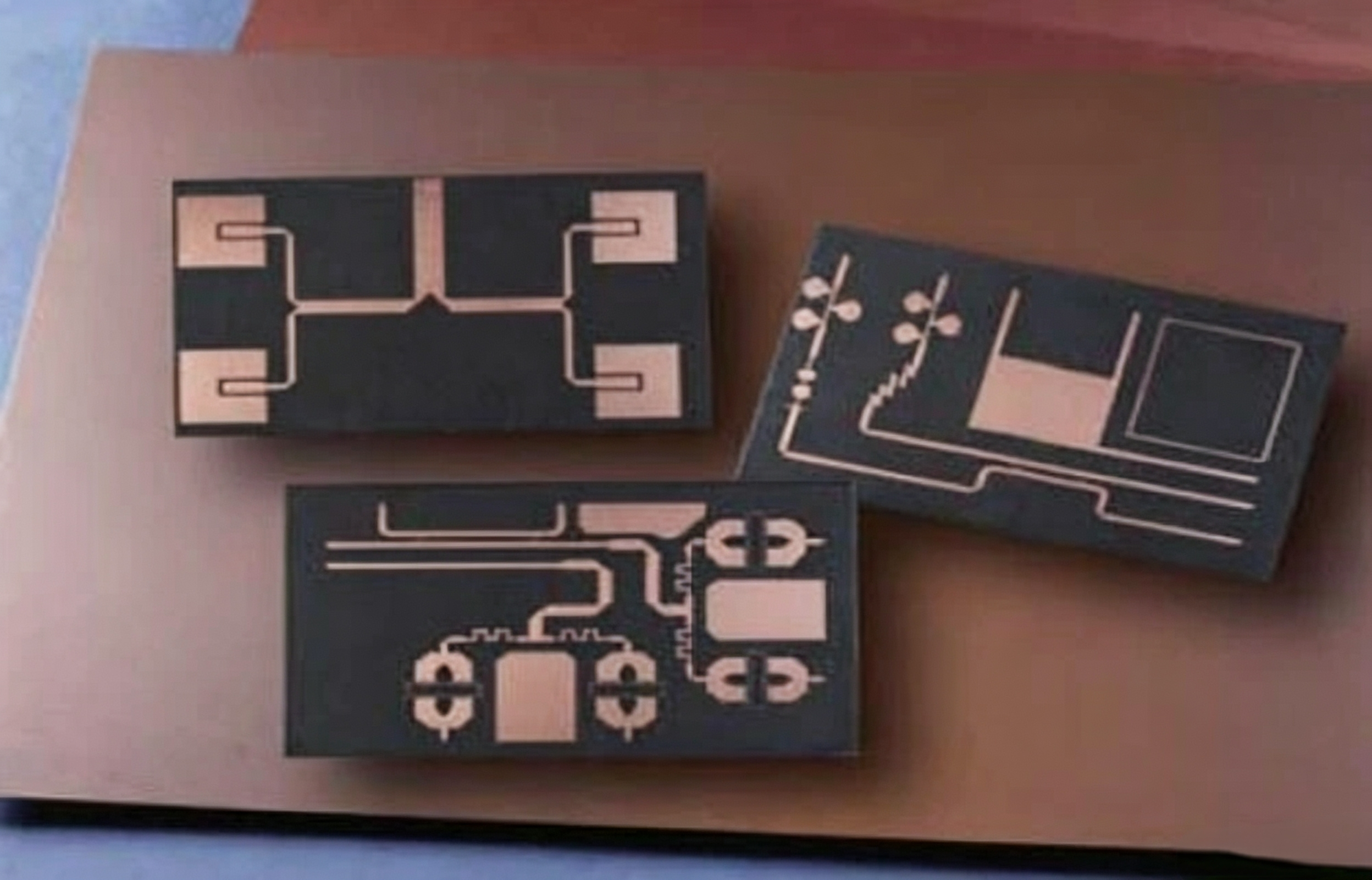
The printed layer is a contact surface as much as a conductor. Wear resistance matters as much as resistance when a rubber key presses against it thousands of times.
Where carbon ink is used
Membrane switch panels are the classic application, including appliance controls and equipment front panels where a sealed interface is required. Remote controls use carbon dots as the contact conductor beneath rubber buttons, which is the highest-volume application of the technology.
Automotive controls follow the same logic: window switches, instrument panel buttons, and seat controls all combine a contact requirement with a long service life. Medical equipment uses carbon ink for disposable diagnostic tools and patient interfaces, and consumer products such as calculators, thermometers, and electronic toys complete the list.
Advantages
Cost is the first advantage. Carbon ink is cheaper than silver-based conductive ink and cheaper than adding copper to carry the same function, which is why it persists in high-volume consumer products. Wear resistance is the second: the printed layer resists oxidation and scratching, which matters when a rubber button presses against it repeatedly.
The process is also simple. Screen printing suits quick prototypes and small batches without the etching and plating steps that a metal layer would require, and the ink can be printed only where it is needed, so the rest of the board is unaffected.
Limits
Contact resistance is the constraint that decides most applications. Carbon ink has a higher resistance than metal, so it is unsuitable for high-current paths and for high-speed signals, where the loss and the impedance change would be unacceptable.
Conductivity is the second limit. Below that of copper or silver, it rules the material out of radio-frequency and power circuits. Print thickness is the third: the ink layer is thicker than a plated conductor, which works against extreme miniaturisation where every micron of profile matters.
Comparing the options
Against silver ink, carbon costs less, conducts less, and is more durable; silver is chosen where the resistance has to be lower. Against conventional copper foil, carbon is cheaper and simpler to process but far less conductive, and copper remains the right answer wherever current or signal speed is the real requirement.
For switch contacts and touch pads, that comparison lands clearly on the carbon side: the requirement is a reliable contact with low wear, and the resistance of the contact is a small part of the circuit. Where the same layer has to carry current or a fast edge, the answer changes. Pad geometry for those contact areas is specified in our guide to PCB pad design standards.

The right question is not which conductor is better, but what the layer actually has to do. A contact and a current path are different jobs.
Manufacturing sequence
The process begins with substrate preparation: cleaning FR-4, polyester, or polyimide so that the ink bonds reliably. The conductive pattern is then screen printed in the required areas, followed by curing at elevated temperature to develop adhesion and conductivity.
Testing follows curing and covers three properties: the resistance of each printed feature, the adhesion of the layer, and the integrity of the printed pattern. Many designs add a protective overprint above the carbon layer to extend its life, and the choice of protective material is a separate decision from the ink itself. The interplay between printable layers and their flow behaviour is described in our guide to solder mask ink thixotropy, and the wider question of protecting a finished assembly is covered under conformal coating for board protection.
Cost and sourcing
The price of a carbon ink PCB depends on the substrate type, the printed area, the batch size, the layer count, and the finish combination. Where a carbon layer is combined with a metallic finish on the same board, both processes have to be planned together, and the precision required for the printed pattern, together with the resistance tolerance, adds cost in proportion to how tight the requirement is.
Compared with silver ink, the total cost is typically lower by a meaningful margin, which is the reason the technique is chosen for high-volume contact products. When selecting a supplier, the questions worth asking are specific: does the shop print carbon regularly, can it hold a defined resistance range, does it test wear and adhesion, does it support quick samples and engineering questions, and is the quotation detailed enough to compare with another supplier?
Sample before production is the last piece of standard advice, and it matters more here than on a conventional board, because contact performance depends on the interaction between the printed surface and the mechanical part that presses against it.
Where the technology keeps appearing
Printed conductors keep finding new applications because they add a function without adding a component. A capacitive touch pad, a battery contact, or an antenna element can be printed in the same pass as the switch contacts, which reduces both the part count and the number of assembly steps. The limit is still the resistance of the layer, so the technique grows wherever contacts and low-current functions are involved and stops where current begins.
FAQ
Can carbon ink carry signal lines? It can carry low-speed, low-current signals where the added resistance is acceptable. It should not be used for high-speed or high-current paths.
How long does the printed layer last? A properly cured layer with an overprint survives millions of actuations, which is why the technique dominates membrane keypads. Wear life depends on the curing profile and on the contact pressure.
Does carbon ink replace the need for a surface finish? No. The metallic areas still need their own finish, and the two processes have to be sequenced so that neither damages the other.