



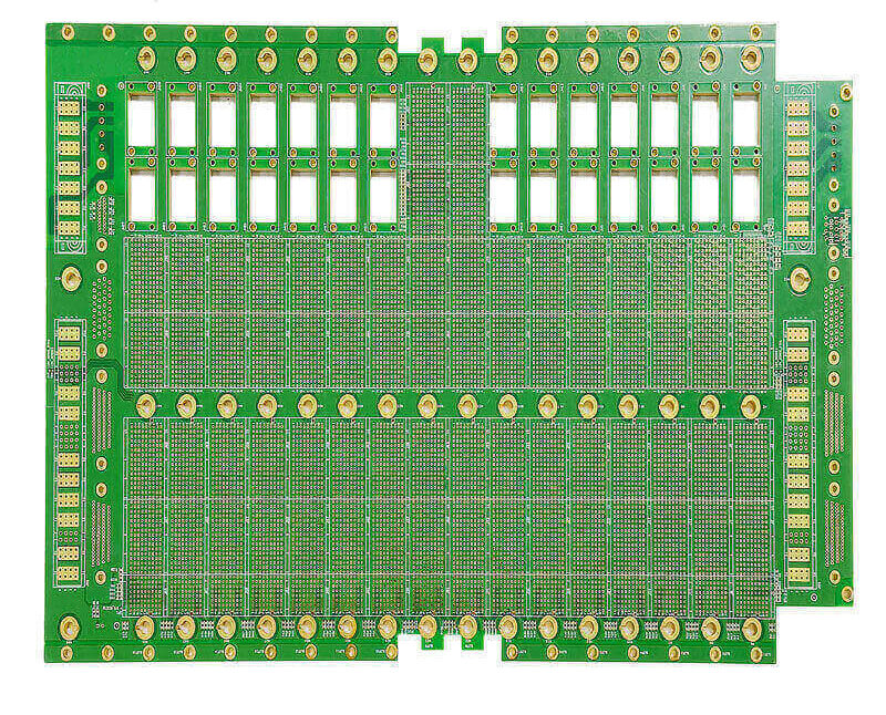
Card Edge Connector and Gold Finger Design
A card edge connector is a board that plugs into a socket, and the contact area is the gold finger. It is a wearing surface, a current path and a mechanical datum at the same time, and it is usually defined by a note rather than by a drawing.
What the Finger Has to Do
The finger carries the signal or the current, it survives the number of insertions the product requires, and it locates the board in the socket so that the contacts line up.
Those functions set the plating, the bevel, the keying and the mechanical tolerances respectively. None of them is decided by the copper thickness alone. Our plating notes describe how the thickness is specified and verified.
Plating System
The finger is usually plated with nickel and then with a thin layer of hard gold. The nickel is the barrier that stops copper diffusion and provides the wear surface underneath; the gold provides the low contact resistance.
A gold layer that is too thin wears through to the nickel, and the contact resistance rises. The specification should state the nickel thickness, the gold thickness and the hardness rather than only the gold.
Bevel and Insertion
The finger needs a bevel so that the socket contact rides onto it rather than catching the edge. The bevel angle and the depth should be defined, because a shallow bevel causes the contact to be lifted and damaged.
The bevel must not cut into the plating that will be in the contact area. The contact zone and the bevel zone should be shown separately on the drawing. Our outline notes describe how the mechanical features are dimensioned.
Keying and Orientation
Keying prevents the board being inserted the wrong way round or into the wrong slot. It can be a notch in the board, a cut-out in the finger area, or a mechanical feature in the housing.
Where the key is a notch, its position and width are mechanical tolerances and they must be controlled to the same level as the finger spacing, or the board will enter at a slight angle and wear unevenly.
Contact Area and Wear
The wear is concentrated where the socket contact sits. The contact area should be defined as a band, and no via, no component and no mask should be within it.
A finger with a via in the contact band has a hole that wears the socket contact, and a finger with mask in the band has a raised area that lifts the contact. Our quality notes describe the inspection that catches both.
Current and Voltage
The current rating of a card edge connector is per contact and it is limited by the socket as well as the board. The board side limit is the copper width and the thickness, because the finger is part of the current path.
Where the voltage is high, the spacing between fingers and the presence of a key become creepage questions rather than mechanical ones. Our current capacity notes describe how the thermal limit is established.
Verification
The verification is a measurement of the plating thickness on a coupon that receives the same plating as the fingers, plus a dimensional check of the bevel, the key and the spacing.
The insertion force should be measured on a sample, because it is the sum of the socket and the board contributions and it changes as the plating wears. Our test coupon notes describe how the coupon is arranged.
Process Control and Verification
On a design of this kind, card edge is the item that decides how the rest of the board is arranged. Reviewing the design before the data is released is cheaper than correcting it after the panel is in the tank, because every step downstream inherits the decision made at the front end. Documenting the assumption is part of the design work, and a short note on the drawing prevents a question that would otherwise arrive a day later and cost a day of schedule.
The process window is set by the narrowest step in the flow, so an improvement anywhere else shows up as margin rather than as yield until that step is addressed. A short note on the drawing about handling, storage or packaging is often worth more than an extra decimal place on a tolerance.
Where a value sits close to a process limit, the drawing should say so, since the shop can then open the process window rather than working to a nominal figure that carries no tolerance. A stack-up that is drawn rather than described removes most of the ambiguity from a quotation, and it lets the fabricator price the board against the dielectric and copper weights that will actually be used.
Where the requirement is not written down, the shop supplies its own default, and the default is chosen for the process rather than for the design.
Process Control and Verification
On a design of this kind, card edge is the item that decides how the rest of the board is arranged. Reviewing the design before the data is released is cheaper than correcting it after the panel is in the tank, because every step downstream inherits the decision made at the front end. Documenting the assumption is part of the design work, and a short note on the drawing prevents a question that would otherwise arrive a day later and cost a day of schedule.
The process window is set by the narrowest step in the flow, so an improvement anywhere else shows up as margin rather than as yield until that step is addressed. A short note on the drawing about handling, storage or packaging is often worth more than an extra decimal place on a tolerance.
Process Control and Verification
On a design of this kind, card edge is the item that decides how the rest of the board is arranged. Reviewing the design before the data is released is cheaper than correcting it after the panel is in the tank, because every step downstream inherits the decision made at the front end. Documenting the assumption is part of the design work, and a short note on the drawing prevents a question that would otherwise arrive a day later and cost a day of schedule.
The process window is set by the narrowest step in the flow, so an improvement anywhere else shows up as margin rather than as yield until that step is addressed.
A first article check confirms that the process and the drawing agree on the points listed above, and that the coupon data supports the values used in the design.
Where a measurement falls outside the expected window, the sample is retained so that the cause can be established before the balance of the batch is released.
FAQ
Can the fingers be plated with the same finish as the rest of the board? They can, but a soldering finish is not a wear surface and it will not survive repeated insertion. The finger is a separate requirement.
Does a longer bevel reduce insertion force? It does, and it also removes more of the edge. The bevel should be defined by the socket it mates with rather than by the force target alone.
What does gopcb provide for card edge fingers? We provide plating specification with nickel and gold thickness and hardness, bevel and contact band definition, keying and orientation features, contact area keep out rules, current and creepage review, coupon based thickness measurement, and insertion force verification.

1 Comment
Connector Thermal Cycling
[…] contact that frets produces an intermittent resistance that is not a solder joint problem. Our card edge notes describe a related wear […]