
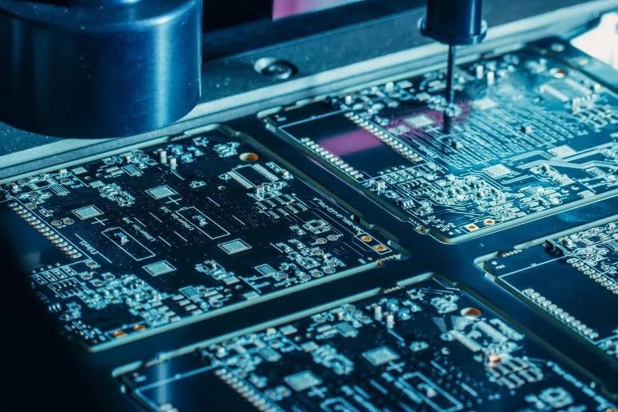
SMT Component Tape and Reel: How the Parts Are Packed Electronics manufacturing has become a discipline of small details. Solder paste volumes, placement accuracy, temperature profiles and inspection limits all add up to the final result. This guide looks at SMT component tape and reel from the perspective of a…
High-Speed PCB Quality Control Standards: A Complete Guide Why High-Speed Boards Need Their Own Controls A conventional digital board tolerates a wide spread in geometry because the signal settles long before the next clock edge. A high speed board does not. A ten percent change in trace width, a 25…
PCB Via Plating Uniformity: Even Copper in the Hole Modern electronics depend on boards that are assembled correctly the first time. Every product – a phone, a charger, a medical instrument or an industrial controller – relies on thousands of solder joints that must conduct current for years. This article…
Wave Soldering vs Reflow Soldering: Which Process to Choose Two Processes, Two Physical Ideas Reflow soldering and wave soldering solve the same problem from opposite directions. Reflow applies heat to a board that already carries solder paste printed on the pads, so the joint forms where the paste was placed.…
PCB Panel Cutting Cost: Equipment, Labor and Material Cutting Sits Between Material and Fabrication Before any circuit is imaged, a copper clad sheet has to be divided into working panels of the size the line can handle. That step looks trivial next to drilling or plating, yet it carries equipment,…
SMT Reflow Solder Paste Slump Test: Checking the Paste Shape Buyers and engineers often focus on the finished product and forget the production line behind it. In practice, most field failures can be traced back to process decisions made during assembly. Understanding SMT reflow solder paste slump test gives you…
HDI 1+N+1 vs 2+N+2: Microvia Stackup Comparison Reading the Notation The numbers in an HDI stackup describe how many build up layers sit on each side of a conventional core. In 1+N+1 there is one microvia layer on the top and one on the bottom, so a via can reach…
PCB Copper Trace Width vs Current: Sizing the Trace to the Load Electronics manufacturing has become a discipline of small details. Solder paste volumes, placement accuracy, temperature profiles and inspection limits all add up to the final result. This guide looks at PCB copper trace width vs current from the…
DIP PCB Assembly Cost in 2026: Price Factors Explained Why DIP Assembly Prices Differ So Much Dual in line packages and other through hole parts are placed and soldered differently from surface mount parts, and that difference is the whole cost story. Where an SMT line places hundreds of components…
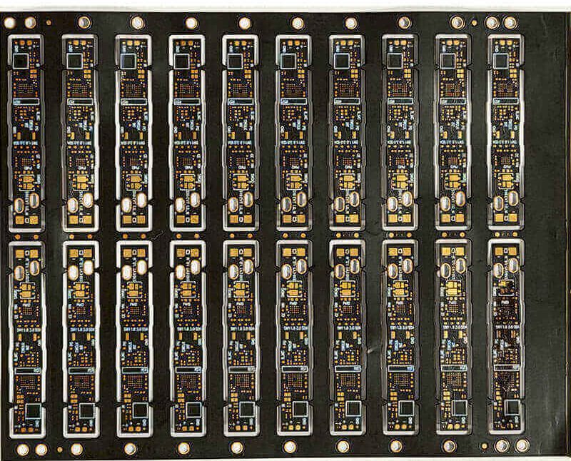
Stamp Hole PCB Cost: Panel Design, Layers and Volume What a Stamp Hole Actually Is A stamp hole edge is a row of small drilled holes left along the outline of a panel so that a sub board can be snapped off by hand or with light tooling. The holes,…